
Index 215
60_DB_GAIN_AT_1_cps_TO_1_MC
Published:2009/7/10 1:37:00 Author:May
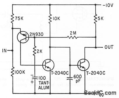
Direct coupled a-c amplifier with feedbock and current defived stabilization uses only two capacitors -P.Lookmann,Direct coupling shrinks Amplifier Size and Cost, Electronics, 36:12, p 66-68. (View)
View full Circuit Diagram | Comments | Reading(590)
COMMON_GATE_MOS_FET
Published:2009/7/10 1:34:00 Author:May
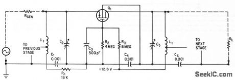
Power gain of 15 db con be obtained from audio up to 200 Mc.-G. G. luettgenau and S. H. Bctmes, Designing With Low-Noise MOS FETs: A Little Different But No Harder, Eletronics, 37:31, p 53-58.
(View)
View full Circuit Diagram | Comments | Reading(666)
Alternating_flasher_using_an_LM3909_chip
Published:2009/7/19 23:58:00 Author:Jessie
Alternating flasher using an LM3909 chip. Circuitry inside the dashes is the LM3909. This circuit is a relaxation oscillator flashing two LEDs sequentially. With a 12-volt DC supply the repetition rate is about 2.5 hertz (courtesy National Semiconductor Corporation). (View)
View full Circuit Diagram | Comments | Reading(892)
SAWTOOTH_CONVERTER
Published:2009/7/10 1:30:00 Author:May
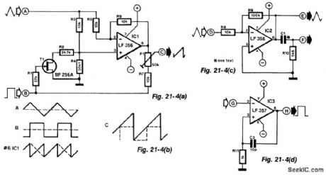
Simple function generators normally provide sinusoidal, rectangular, and triangular waveforms, but seldom a sawtooth. The circuit in Fig. 21-4(a) derives a sawtooth signal from a rectangular and triangular signal. Its quality depends on the linearity of the triangular signal, the slope of the edges of the rectangular signal and the phase relationship between the rectangular and triangular signals.
The conversion is carried out in IC1. Whether the triangular signal at input A is converted or not by IC1 depends on the state of T1. This FET is controlled by the rectangular signal at input B.
The signal at the output of the op amp is a sawtooth (see Fig. 21-4(b)) whose trailing edge is inverted. The frequency of this signal is double that of the input signals.
If in this state, the dc level of each inverted edge is raised sufficiently to make the lower level of that edge coincide with the higher level of the preceding edge, a sawtooth signal of the same frequency (but double the peak value of the input signals) is obtained. The dc level is raised by adding input B to the output of IC1 via R7 and P1. The preset should preferably be a multiturn type. Resistors R2 and R4 are 1% types.
If a rectangular signal is not available, or if its peak value is too small, the auxiliary circuits (shown in Figs. 21-4(c) and 21-4(d)) will be found useful. Figure 21-4(g) amplifies the triangular input at A by 10. Differentiating network C1/R10 derives rectangular pulses from the amplified triangular signal and these are available at F.
The pulses at F are shaped by the circuit in Fig. 21-4(d) to rectangular signals that have the same peak value as the supply voltage. Capacitor C2 increases the slope of the edge; it can be omitted for low-frequency signals.
The converter provides sawtooth signals over the frequency range of 15 Hz to 15 kHz. If the auxiliary circuits are used, capacitor C1 must be compatible with the frequency of the sawtooth signal (its value lies between 2 nF and 100 pF). The supply for all circuits can be between ±10 V and ±15V. Each op amp draws a current of 4 to 6 mA. (View)
View full Circuit Diagram | Comments | Reading(1372)
Automatic_flasher_light_for_use_around_marine_buoys_piers_or_towers
Published:2009/7/19 23:54:00 Author:Jessie
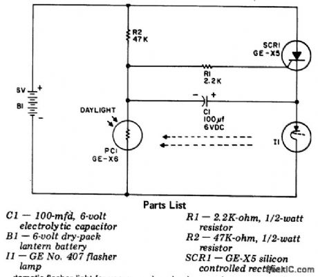
Automatic flasher light for use around marine buoys, piers, or towers. It starts working at dark and stops at dawn. When constructing this circuit be sure to place the photoresistor so that it receives as much light as possible without interfering with the flasher light (courtesy General Electric Company). (View)
View full Circuit Diagram | Comments | Reading(587)
SIGNAL_INJECTOR
Published:2009/7/10 1:29:00 Author:May
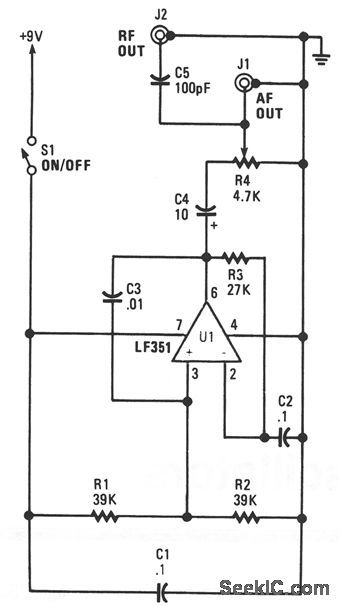
This unit is a single oscillator built around an LF351 JFET-input op amp. Resistors R1 and R2 bias the noninverting input while R3 biases the inverting input from the output. This layout provides 100% negative feedback, but the decoupling caused by C2 gives reduced feedback and high-voltage gain when dealing with audio frequencies. The fundamental operating frequency is about 800 Hz. Potentiometer R4 is the output-level control. To use it start at the speaker. If no tone is heard, move back to the amplifer input, and listen for the tone. Still if no tone is heard, continue backtracking from the output to the input, covering all stages in between. The stage where the signal is lost is the one that is not operating. (View)
View full Circuit Diagram | Comments | Reading(1393)
ELECTRONIC_DOORBELL
Published:2009/7/10 1:29:00 Author:May
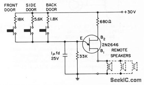
Single unijunctfon transistor oscillates at different tone for each door.- Tronsislor Manucl, Seventh Edition, General Electric Co., 1964, p 380.
(View)
View full Circuit Diagram | Comments | Reading(560)
Continuous_indicator_using_an_LM3909_chip
Published:2009/7/19 23:53:00 Author:Jessie
Continuous indicator using an LM3909 chip. Circuitry inside dashes is the LM3909. The circuit actually flashes at a 2 kHz rate, which cannot be detected by the human eye. This indicator is not intended as a long life system since current drain is 12 mA (courtesy National Semiconductor Corporation). (View)
View full Circuit Diagram | Comments | Reading(579)
FLAT_TV_GENERATOR_MODULATOR
Published:2009/7/19 23:52:00 Author:Jessie
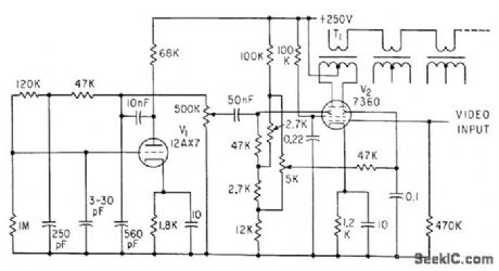
R-C gen erator V1, generating one of nine differ. ent carrier frequencies, feeds defection plate of beam deflection tube V2, while video modulation from camera is fed to grid 1 of V2 to modulate the carrier.-B. Binggeli and E. Fatuzzo, Solid-State Panels: Will They Bring Flat-Display TV?, Electronics, 35:26, p 67-70. (View)
View full Circuit Diagram | Comments | Reading(714)
The function features of TOPSwitch—Ⅱ
Published:2011/7/20 23:27:00 Author:Borg | Keyword: function features, TOPSwitch—Ⅱ
The features of the TOPSwitch—Ⅱproducts:(1) all the functions of PWM control system are combined on the 3-terminal chip, which contains the PWM, power switch MOSFET, auto bias circuit, protection circuit, high voltage starting circuit and circuit compensation circuit, the output terminal and the grid are fully separated by the HF transformer, so the single chip integration of the auto frequency transformer, separator and reversed motivation switch power is completed, which is safe and reliable. (View)
View full Circuit Diagram | Comments | Reading(575)
PROGRAMMABLE_INVERTER_RECTIFER
Published:2009/7/10 1:23:00 Author:May
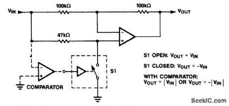


The op amp is alternately an inverter or buffer, under control of the switch polarity. As a buffer, the gain is always 1, but as an inverter, the gain is set by the ratio of the input and feedback resistors. By adding a comparator, the function can be synchronously switched as the input polarity changes, which ffectively rectifies the output. The output polarity is determined by the switch logic (normally open or normally closed) and the comparator input polarity. (View)
View full Circuit Diagram | Comments | Reading(757)
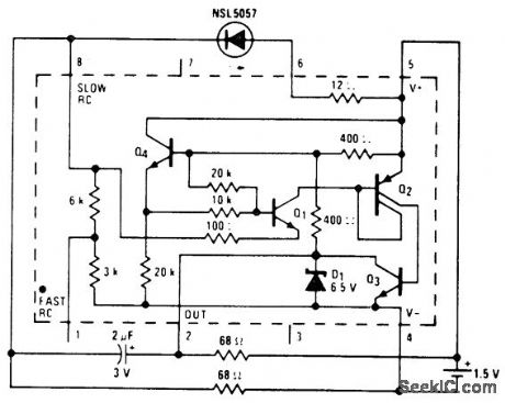
MULTIPLE_APERTURE_WINDOW_DISCRIMINATOR
Published:2009/7/10 0:59:00 Author:May
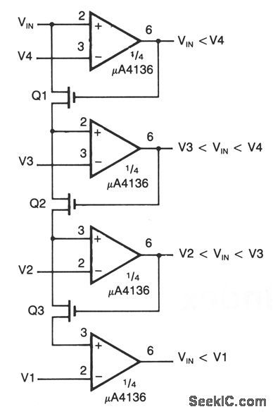
The circuit shown here uses μA4136 comparators and FETs Q1 through Q3. (View)
View full Circuit Diagram | Comments | Reading(2047)
COMPOUND_OP_AMP_VCO_DRIVER
Published:2009/7/10 0:57:00 Author:May
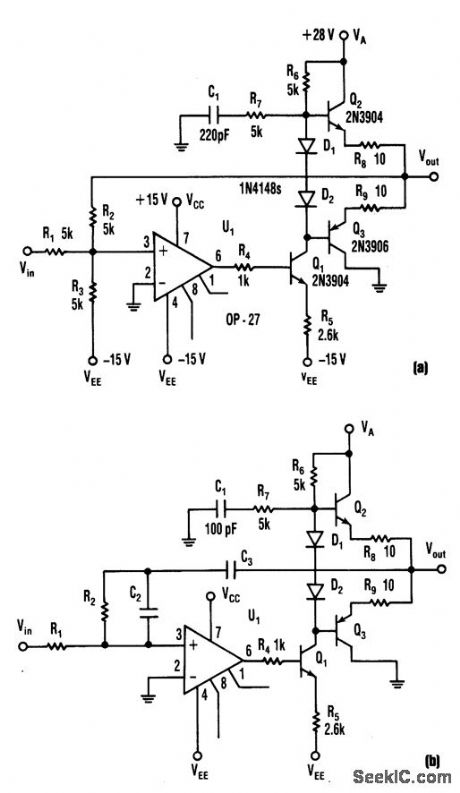
This circuit produces 5-to 25-V output to drive a VCO from a standard ±15-V supply system. R7 and C1 supply frequency compensation. Q1 through Q3 form an inverting amplifier with a gain of two.Negative feedback through R2 closes the loop. This circuit can act as a an active load-log filter and directly drive a voltage-controlled oscillator. (View)
View full Circuit Diagram | Comments | Reading(857)
SAMPLE_AND_HOLD
Published:2009/7/10 0:56:00 Author:May
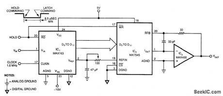
By using the ADO and DAC, this circuit uses a negative pulse to latch data into the ADO. The hold pulse width should be at least 8.5 μs. This circuit has zero drop and infinite hold time. (View)
View full Circuit Diagram | Comments | Reading(0)
RF_UPCONVERTER_FOR_TVRO_SUBCARRIER_RECEPTION
Published:2009/7/10 0:54:00 Author:May
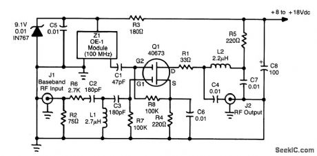
This converter uses a 40673 MOSFET to heterodyne the 5.5- to 8-MHz TVRO subcarriers to the FM broadcast band, where a stereo receiver can be used for high-fidelity stereo reception of TV sound subcarriers. 21 is a prepackaged 100-MHz oscillator module, which is available from International Crystal Corporation, Oklahoma City, Ok. (View)
View full Circuit Diagram | Comments | Reading(652)
220_MHz_RECEIVING_CONVERTER
Published:2009/7/10 0:53:00 Author:May
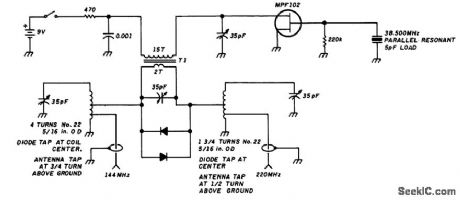
A simple circuit using a single transistor converts 220 MHz to 144 MHz or vice versa, because the mixer is bilateral. T1 has 15 turns on the primary, and 2 turns on the secondary (#24 AWG wire) on a 0.375 ID SF-material toroidal coil. (View)
View full Circuit Diagram | Comments | Reading(1561)
SHORTWAVE_CONVERTER_FOR_AM_CAR_RADIOSS1_
Published:2009/7/10 0:52:00 Author:May
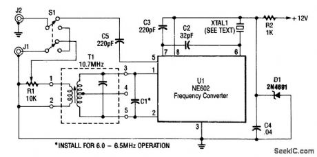
Using a Signetics NE602, this converter tunes the 9.5- to 9.8-MHz range. An AM car radio is used as a tunable IF amplifier. Output is taken from J2, the auto antenna. The crystal (XTAL1) can be a frequency about 1 MHz below the desired tuning range; for 9.5 to 9.8 MHz, an 8.5- to 8.8-MHz crystal should be used. (View)
View full Circuit Diagram | Comments | Reading(2469)
10_MHz_WWV_TO_80_METER_SW_CONVERTER
Published:2009/7/10 0:50:00 Author:May
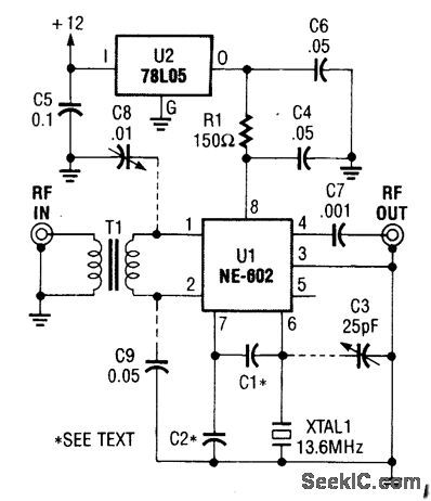
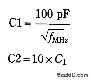

This converter is useful where reception of WWV is desirable and only a ham-band receiver is available. U1 acts as a mixer/oscillator. The values of C1 and C2 are given by: (View)
View full Circuit Diagram | Comments | Reading(640)
RECEIVER_FREQUENCY_CONVERTER_STAGE
Published:2009/7/10 0:48:00 Author:May
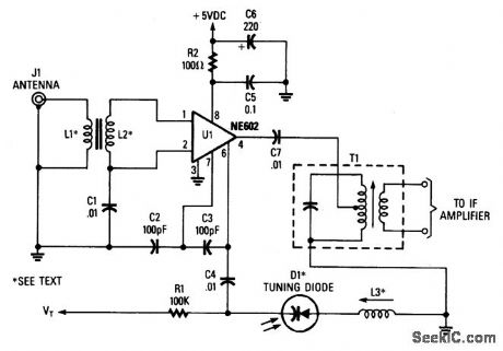
L1, L2 1:12 Tums Ratio Toroid (Broadband).L3 Resonates to L.0. Frequency with D1 capacitance.LO FREQ Desired received frequency ± IF frequency.In this case, the NE602 is used in this superhet front-end configuration. U1 serves as a frequency converter. L1/L2 is a broadband toroidal transformer. A tuned transformer may be used instead. The sup-ply voltage is +5 to +9 Vdc. T1 is tuned to the IF frequency. The typical IF frequency is 455 kHz. This circuit, depending on L1, L2, and L3, should be usable in the frequency range from audio to 30 MHz. The varactor tuning diode can be replaced with an air-variable capacitor, if desired. (View)
View full Circuit Diagram | Comments | Reading(969)
2_METER_CONVERTER
Published:2009/7/10 0:47:00 Author:May
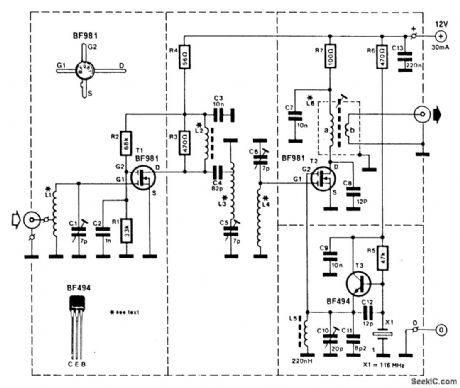
This converter enables a receiver that tunes 28 to 32 MHz to receive the 144- to 148-MHz amateur band. A BF981 dual-gate MOSFET provides RF gain and feeds mixer T2, another BF981. T3 is a 116-MHz crystal oscillator used to provide L.O. injection to T2. Coils are wound on a 6-mm form. L1, L3, and L4 are 8 turns of 1-mm diameter silver-plated copper wire. L2 is 4 turns of 0.2-mm wire through a ferrite lead. L6 has 19 turns on the primary and 3 turns on the secondary. (View)
View full Circuit Diagram | Comments | Reading(6081)
| Pages:215/471 At 20201202203204205206207208209210211212213214215216217218219220Under 20 |
Circuit Categories
power supply circuit
Amplifier Circuit
Basic Circuit
LED and Light Circuit
Sensor Circuit
Signal Processing
Electrical Equipment Circuit
Control Circuit
Remote Control Circuit
A/D-D/A Converter Circuit
Audio Circuit
Measuring and Test Circuit
Communication Circuit
Computer-Related Circuit
555 Circuit
Automotive Circuit
Repairing Circuit