
Index 208
VOLTAGE_TUNED_60_TO_90_MC
Published:2009/7/10 5:07:00 Author:May
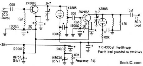
Gives over 40 db gain with 50-ohm source and load.Untuned input allows constant source impedance over tunable frequency range of silicon XA585 voltage-variable capacitance diodes, with excellent stability and trctcking.-Texas Instruments Inc., Solid-Stale Communications, McGraw-Hill, N.Y., 1966, p 297.
(View)
View full Circuit Diagram | Comments | Reading(549)
BIDIRECTIONAL_INTERCOM_
Published:2009/7/10 5:06:00 Author:May
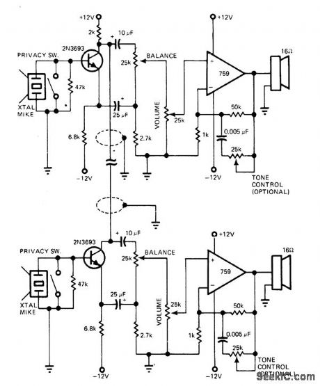
Uses 759 power opamps to provide 0.5 W for 16-ohm loudspeakers. Crystal microphones feed NPN transistors that provide both inphase and 180o out-of-phase signals. Balance-adjusting circuits of am-plifiercancel outthe two signals, so only out-ofphase sigpal goes to receiving unit. Privacy switch across microphone eliminates audio feedback while listening. Artide tells how to calculate heatsink requirements.-R. J. Apfel, Power Op Amps-Their lnnovative Circuits and Packaging Provide Designers with More Options, EDN Magazine, Sept. 5, 1977, p 141-144. (View)
View full Circuit Diagram | Comments | Reading(1122)
HIGH_GAIN_VOLTAGE_STABILIZER
Published:2009/7/10 5:03:00 Author:May
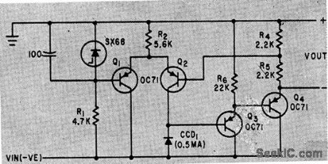
Use of constant-currenl diode as collecfor load increases overall gain of amplifier from 500 to about 700.-T. K. Hemingway, Applications of the Constant-Current Diode, Electronics, 34:42, p 60-63. (View)
View full Circuit Diagram | Comments | Reading(546)
BATTERY_TRIGGERED_ac_SWITCH
Published:2009/7/10 5:02:00 Author:May
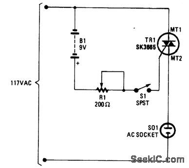
Using this method, a small switch (S1) can con-trol a large ac load. R1 is adjusted for reliable trig-gering and should be as large as possible. (View)
View full Circuit Diagram | Comments | Reading(626)
DIVIDE_BY_2_OR_3_CIRCUIT
Published:2009/7/10 5:01:00 Author:May
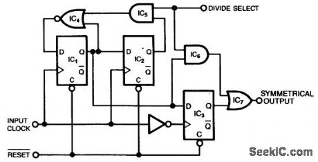
This circuit produces a symmetrical waveform when dividing by either 2 or 3. The Divide Select input controls the division factor. When Divide Select is high, flip-flops IC1 and IC2, along with associated gates, form the classical divide-by-3 circuit.
When divide select is low, however, the output of the AND gate, IC5, goes low. Consequently, the NOR gate, IC4, inverts the feedback signal and passes it to the D input of the flip-flop, IC1. Now, IC1 acts like a toggle flip-flop and produces a divide-by-2 output.
IC3, which is, in effect, a negative-edge-triggered flip-flop, provides symmetrical output signals. When you select division by 2 (Divide Select is low), the output and AND gate IC6 is low, and IC3 simply clocks out the divider's output, delayed by one clock period. When you set Divide Select high, the path to the output through the AND and OR gates, IC6 and IC7, is enabled. This path means that the output goes high on the leading edge of IC3's input (not its output) and produces a symmetrical divide-by-3 output. (View)
View full Circuit Diagram | Comments | Reading(1169)
7490÷N_CIRCUITS
Published:2009/7/10 5:01:00 Author:May
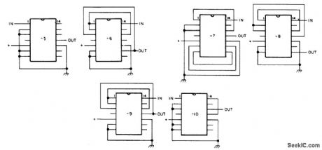
A 7490, 74LS90, 74C90, etc., is a decode divider, but it can be configured to divide by any N up to 10. The above figures illustrate the connections necessary to divide by N from 5 to 10. (View)
View full Circuit Diagram | Comments | Reading(3458)
BEEPER
Published:2009/7/10 5:00:00 Author:May
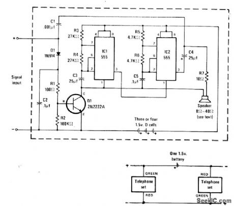
Private two-station telephone system for home requires only two wires between ordinary telephone sets, with 1.5-V battery in series with one line, but this voltage is not enough to actuate ringers in sets.Beeper in parallel with each set, with polarity as shown, serves same purpose as ringer. 555 timer IC1 turns on IC2 about once every 3 s, and IC2 then generates 1000-Hz beep for about 1 s as ringing signal. No switches are required, because telephone handsets provide automatic switching.When both telephones are hung up, 1.5-V battery splits equally between beepers and resulting 0.75 V is not enough to turn on Q1 in either set. When one telephone is picked up, beeper at other telephone receives close to 1.5 V and Q1 turns on IC1 to initiate beeping call. When other telephone is picked up, beeping automatically stops because 1.5 V is again divided between sets.-P. Stark, Private Telephone: Simple Two-Station Intercom, Modern Electronic, July 1978, p 32-34. (View)
View full Circuit Diagram | Comments | Reading(0)
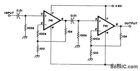
STABILIZING_GAIN
Published:2009/7/10 4:55:00 Author:May
Use of negative feedback in four-stage direct-coupled amplifier keeps gain constant within 1 db of 40 db from 6 cps to 300 kc. Input impedance is 8 meg end output impedance is 600 ohms.-Feed-back Increases Input Impedance, Electronics, 32:11, p 150-153. (View)
View full Circuit Diagram | Comments | Reading(526)
2_W_WITH_IC
Published:2009/7/10 4:54:00 Author:May
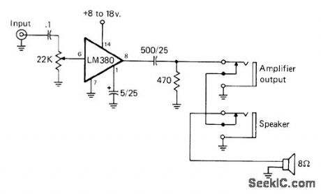
lnexpensive audio amplifier using 14-pin DIP provides adequate power for small audio projects and audio troubleshooting.Pins 3, 4, 5, 10, 11, and 12 are soldered directly to foil side of printed-wiring board used for construction,to give effect of heatsink.-J. Schultz, An Audio Circuit Breadboarder's Delight, CQ, Jan. 1978, p 42 and 75. (View)
View full Circuit Diagram | Comments | Reading(1408)
PROGRAMMABLE_FREQUENCY_DIVIDER
Published:2009/7/10 4:54:00 Author:May
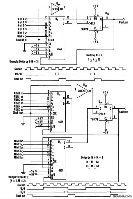
This divider uses a variable-length shift register, a type-D flip-flop, and an inverter. The clock feeds the flip-flop clock input and the output of the shift register feeds the D input of the flip-flop. The FF output is tied back to the reset input of the shift register so that each clock pulse shifts a 1 into the 4557. N+ 1 cycles after the reset pulse is removed. The first 1 will propagate through the register output. The 1 is latched into the FF on the clock's next falling edge and fed back to the 4557 reset pin, which resets the shift register to zero. When a zero is clocked into the flip-flop on the next falling clock edge, the reset is removed, restarting the process. The divide ratio is (N+2), where N = the binary number that is programmed into 4557. (View)
View full Circuit Diagram | Comments | Reading(1510)
ELECTRONIC_ANTENNA_SELECTOR
Published:2009/7/10 4:54:00 Author:May
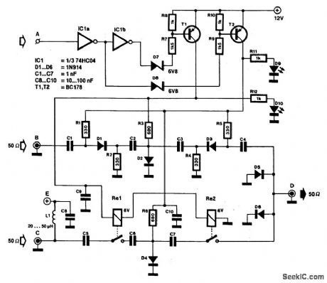
The electronic antenna selector is intended to switch between two FM antennas via a logic signal. Gates IC1A and IC1B ensure a clean switching action and at the same time form the interface between the 5-V logic level (probably available from the receive) and the 12-V supply voltage for the selecton Depending on the type of gate used, a digital TTL or CMOS control signal is available in direct and inverted form at the outputs of IC1.When input A is logic high, the output of IC1A is low and that of IC1B is high. The current then flows from the positive supply line to IC1A via T2, R9, and D8. T2 is switched on and D9 lights.Because direct currents flow through R1/D1/R2 and R5/D3/R4, diodes D1 and D3 conduct and pass the VHF signal from input A to output D. At the same time, a direct current flows through R6/D4 so that D4 conducts. This arrangement ensures that any VHF signal at input C cannot reach the output via the parasitic capacitances of the relay contacts and the wiring.When A is logic low, and IC1B is therefore low, the current flows from the positive supply line to IC1B via T1, R7, and D17. T1 is then switched on and D10 lights. At the same time, the two series-connected relays, Re1 and Re2, are energized, their contacts close, and the VHF signal at input C is fed to output D. Moreover, a direct current flows through R3/D2 so that D2 conducts. Any signal at input B is then shorted to ground via D2.All resistors should be carbon-film types because these have a higher parasitic series inductance than metal-film resistors. Thus, the attenuation of the VHF signal caused by them is reduced to a minimum.The attenuation losses caused by the diode junctions (5-10 dB) are somewhat larger than those caused by the relays. It is thus advisable to connect the antenna that provides the weaker signal (normally the domestic one) to input C. If the domestic antenna is equipped with an antenna amplifier, it can be supplied via terminal E. Diodes D5 and D6 protect the circuit against high-voltage spikes that occur during the on and off switching. The selector draws a current of approximately 65 mA. (View)
View full Circuit Diagram | Comments | Reading(765)
CLOCK_INPUT_FREQUENCY_DIVIDER
Published:2009/7/10 4:50:00 Author:May
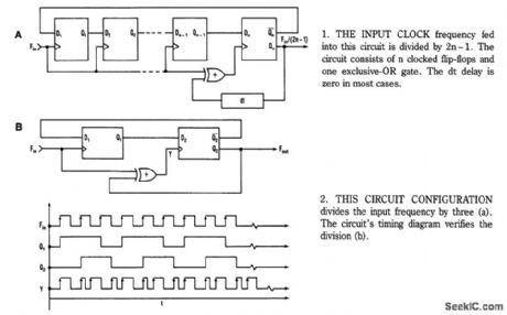

ICA, R1 through R3, and Q1 form a current source. The current that charges C1 is given by:
The input signal drives ICD. Because ICD's positive input (V+) is slightly offset to +0.1 V, its steady-state output will be near + 13 V. This voltage is sent to ICC through D2, setting ICC's output to +13 V. Therefore, point D is cut off by D1, and C1 is charged by the current source. Assuming the initial voltage on C1 is zero, the maximum voltage (I/Cmax) is given by:
The right side of the inequality should be the minimum pulse width (either up time or down time) of the input clock. The circuit, when constructed with standard 74F-type parts, operates without any added delay in the exclusive-0R feedback path and with an input frequency of up to 22.5 MHz. The circuit's output signal will have the same duty cycle as the input clock. (View)
View full Circuit Diagram | Comments | Reading(1026)
BIPOLAR_INPUT_FOR_V_F_CONVERTER
Published:2009/7/10 4:35:00 Author:May

Absolute-value integrator circuit gives effect of generating negative frequencies when input signal is negative by making counter count up for positive voltage and count down for negative voltage. Diode types are not criticaL-M. O. Paiva, Applications of the 9400 Voltage to Frequency Frequency to Voltage Converter, Teledyne Semiconductor, Mountain View, CA, 1978, AN.10, p 3. (View)
View full Circuit Diagram | Comments | Reading(673)
LATCHING_CONTINUITY_CHECKER
Published:2009/7/10 4:32:00 Author:May
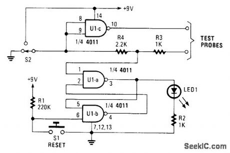
This circuit detects brief shorts or opens. When S2 is in the up position, the circuit indicates if there is or was continuity by lighting LED1. U1A and U1B are connected as an R-S flip-flop. S1 resets the tester.When S2 is in the down position,a momentary interruption in continuity will light LED1.This tester is good for detecting intermittent shorts or opens. (View)
View full Circuit Diagram | Comments | Reading(701)
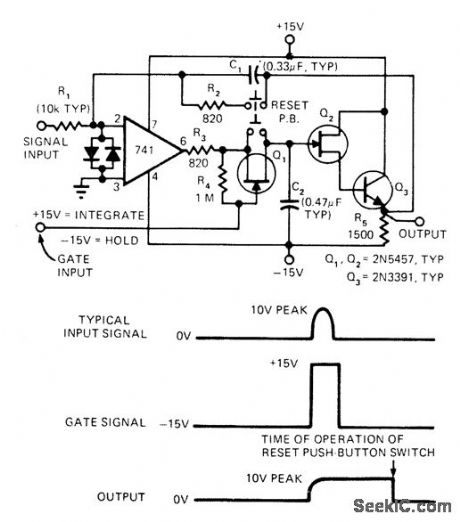
LOGIC_RESETTABLE
Published:2009/7/10 4:31:00 Author:May
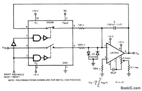
DG200 CMOS analog switch serves for discharging integrator capacitor C rapidly for high logic input pulse, Other section of switch disconnects integrator from analog input when logic goes high. When logic input is returned to low, integrator is triggered. Diodes prevent capacitor from charging to over 15V.- Analog Switches and Their Applications, Siliconix, Santa Clara, CA, 1976, p 7-68. (View)
View full Circuit Diagram | Comments | Reading(774)
BASIC_MULTIVIBRATOR
Published:2009/7/10 4:31:00 Author:May
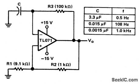
When this circuit is turned on, the natural offset of the devices serves as an automatic starting voltage.Assume that output voltage VO goes positive and the positive feedback through R2 and R1 forces the out-put to saturate. The high-voltage level at VO, then charges C through R3, until the voltage at the inverting input exceeds that at the noninverting input.As the inverting input exceeds the noninverting input level, the output switches to the negative saturation voltage. This action starts the capacitor discharging toward the new noninverting input level. When the capacitor reaches that level, the op amp switches back to the positive saturation voltage, and the process starts again. With the TL071, the positive and negative output levels are nearly equal, which results in a 50% duty cycle. The total time period of one cycle will be: (View)
View full Circuit Diagram | Comments | Reading(678)
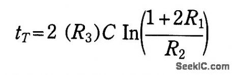
DIGITAL_COMPASS
Published:2009/7/10 4:29:00 Author:May
A four output Hall sensor combined with a few logic gates produce this digltal compass. The NOR gates resolve the four Hall outputs into eight distinct compass directions. LEDs to indicate direction aredriven by eight inverters. A power supply for 5.25-to 18-Vdc operation IS shown in the figure. (View)
View full Circuit Diagram | Comments | Reading(1963)
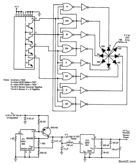
Sample_and_hold_circuit_with_Av_=___1
Published:2009/7/19 20:13:00 Author:Jessie
Sample-and-hold circuit with Av = + 1. The chip is an AD582 sample-and-hold amplifier (courtesy Analog Devices, Inc.). (View)
View full Circuit Diagram | Comments | Reading(706)
ANALOG_START_STOP_AND_RESET
Published:2009/7/10 4:26:00 Author:May
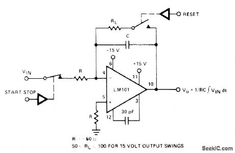
One section of DG300 dual analog switch serves for discharging integrator capacitor C through RL when resetting integrator, with start/stop switch section being held open by control logic.When both switches are open, output of integrator is held.- Analog Switches and Their Applications, Siliconix, Santa Clara, CA, 1976, p7-81. (View)
View full Circuit Diagram | Comments | Reading(2049)
RMS_CONVERTER
Published:2009/7/10 4:23:00 Author:May
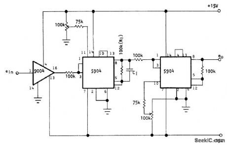
Converts analog voltage to RMS equivalent by squaring operation followed by integration and squarerooting. Bipolar input signal is first converted into linear absolute value with Optical Electronics 9004 absolutevalue module, as required for processing by 5904 unipolar devices. Pots are used to establish 10-V full-scale level.R1C1is integration time constant.- Simple RMS Converter, Optical Electronics, Tucson, AZ, Application Tip 10246. (View)
View full Circuit Diagram | Comments | Reading(943)
| Pages:208/471 At 20201202203204205206207208209210211212213214215216217218219220Under 20 |
Circuit Categories
power supply circuit
Amplifier Circuit
Basic Circuit
LED and Light Circuit
Sensor Circuit
Signal Processing
Electrical Equipment Circuit
Control Circuit
Remote Control Circuit
A/D-D/A Converter Circuit
Audio Circuit
Measuring and Test Circuit
Communication Circuit
Computer-Related Circuit
555 Circuit
Automotive Circuit
Repairing Circuit