
Index 216
VLF_CONVERTER
Published:2009/7/10 0:45:00 Author:May
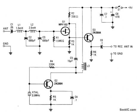
The VLF Converter can be used to pick up signals for the general coverage of shortwave receivers. A number of unusual signals can be heard on frequencies below 15 kHz.This converter wiil convert frequencies from 0 to 250 kHz to 3500 to 3750 kHz so that the LF- and VLF-band segments can be received on an amateur or shortwave receiver that covers 3 500 to 4000 kHz.Signals from a short whip antenna (8 to 10 feet) are coupled through low-pass filter L1/L2/C2/C3 to RF amp Q1. Q3 mixes these signals with a 3.5-MHz signal from Q2 and associated components C4, R5, R4, and 3.5-MHz XTAL. L3 is an RF choke that presents an inductive load to Q3. It should be resonant some-what above 3.5 MHz when placed in the circuit. An adjustable coil of about 30 to 100 μH should be suffi-cient. The converter output is taken from the emitter of Q3 through C6. (View)
View full Circuit Diagram | Comments | Reading(7702)
LOW_NOISE_420_MHz_ATV_RECEIVER_CONVERTER
Published:2009/7/10 0:44:00 Author:May
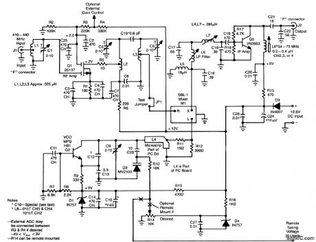
L1, Q1, L2,and L3 compose an RF amp⒒fter stage that feeds Ml,a doubly balanced mixer. Q4 is alocal oscillator stage In the 375-MHz range.Signals h the 420ˉto 450-MHz range from Q1 are mixed in M1 and fed through filter L6/L7/C17,where only the 60- to 70-MHz (CH3/CH4) signals pass. The IF signal is passed to Q3, an IF amplifier. The overall gatrns 25 dB and the noise figure less than 2 dB. A kit of all parts,including the PC board,is available from North Country Radio, P.O. Box 53,Wykagyl Station,New Rochelle,NY 10804. (View)
View full Circuit Diagram | Comments | Reading(929)
DIGITAL_FREQUENCY_WINDOW
Published:2009/7/10 0:39:00 Author:May
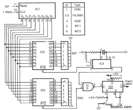
This circuit detects frequency variation above or below preset limits. IC1 is a binary counter clocked at FCLK. The outputs are compared with switch preset values by IC2 and IC3. The input signal, which must be a positive-going pulse, is used to reset IC1. The P greater than Q output of the comparators is at logic 0 for input frequencies below the preset values. Above the preset count, a pulse train is output.IC2, detects a low input by supplying the pulse train to a retriggerable monostable, IC4. When the input frequency falls below the preset value in SW1, the monostable is no longer triggered and its output falls to logic 0. IC3 detects the frequency high state SW2, and outputs directly when this occurs. The outputs from both comparators can then be latched as shown, using IC5 and IC6. The clock frequency is related to input and switch values: switch value = FCLK/input. The time constant of IC4 is not critical, but must obviously exceed the maximum input pulse period. (View)
View full Circuit Diagram | Comments | Reading(837)
RADIO_BEACON_CONVERTER
Published:2009/7/10 0:39:00 Author:May
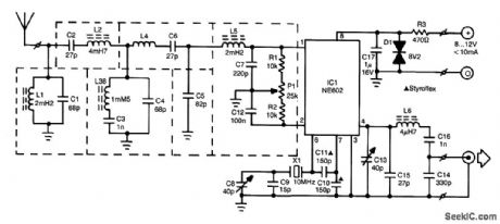
The radio beacon band extends from 280 to 516 kHz. Each beacon has its own characteristic AM-modulated morse-coded callsign that is transmitted on a specific frequency. To be able to receive distant beacons, the aerial signal is passed through a band-pass filter that effectively suppresses longwave and mediumwave signals. The ftlter also converts the aerial impedance, Zin, from about 10 kΩ to the input impedance of mixer IC1, which is about 1 kΩ.The mixer adds or subtracts the received signal to/from the local oscillator signal so that the beacon signal can be received on a normal shortwave receiver. The resulting frequencies are from 9.72 to 9.48 MHz or from 10.280 to 10.516 MHz. In the construction of the converter, some components must be surrounded by a metal shield, as indicated by dashed lines on the PC board layout.The circuit is aligned with the aid of an SSB receiver, to which the output of the convener is con-nected. Tune the receiver to 10 MHz and adjust the oscillator frequency of the converter with C8 for zero beat. Next, detune the receiver slightly until you hear a pleasant whistle, which is adjusted for minimum level with the aid of Pl. Finally, tune to a beacon transmitting at or about 300 kHz and adjust C13 for maximum sound output. (View)
View full Circuit Diagram | Comments | Reading(2112)
FACSIMILE_SWEEP_AMPLIFIER
Published:2009/7/20 1:46:00 Author:Jessie
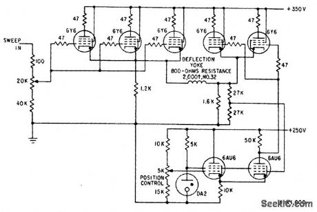
Provides power amplification for driving electronic high-definition facsimile recorder. Sweep input voltage is high enough to eliminate need for voltage gain in power amplifier stages.-E. W. Van Winkl, High-Precision Sweep Generator, Electronics, 33:50. p 88-90. (View)
View full Circuit Diagram | Comments | Reading(572)
SIMPLE_TESLA_COIL
Published:2009/7/10 0:28:00 Author:May
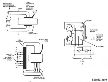
The Tesla coil described here can generate 25,000 V. So, even though the output current is low, be very careful! The main component is a flyback transformer from a discarded TV.A new primary winding is needed. Begin by winding 5 turns of #18 wire on the core. Then, twist a loop in the wire, and finish 'ay winding five more turns. Wrap with electrical tape, but leave the loop exposed.A four-turn winding must be wound over the ten-turn winding that you've just finished. That is done the same way. First wind two turns of # 18 wire, then make a loop, and finish by winding two more turns.Again, wrap the new winding with electrical tape, leaving the loop exposed.When the windings are finished, the two loops shouldn't be more than 1/4-inch apart, but take care that they do not touch. Connect a 240-Ω resistor between the two loops. The modified transformer now should look like the one shown. Connect the transformer as shown. The 27-Ω resistor and two transistors should be mounted on a heatsH and must be insulated from it.The output of the high-voltage winding should begin to oscillate as soon as the circuit is connected to a 12-Vdc power supply. If it does not, reverse the connections to the base leads of the transistors. In normal operation, you should be able to draw 1-inch sparks from the high-voltage lead using an insulated screw-driver. (View)
View full Circuit Diagram | Comments | Reading(3692)
RAIL_FAULTDETECTING_AMPLIFIER
Published:2009/7/20 1:44:00 Author:Jessie
Signals from inductive pickup near rail are amplified enough to drive sensitive relay of pen recorder. Amplifier does not block after being overloaded when pickup passes over rail joint.-H. W. Keevil, Transistor Pulse Amplifiers Detect Rail Faults, Electronics, 35:21, p 53-54. (View)
View full Circuit Diagram | Comments | Reading(635)
CURRENT_TO_FREQUENCY_CONVERTER
Published:2009/7/10 Author:May
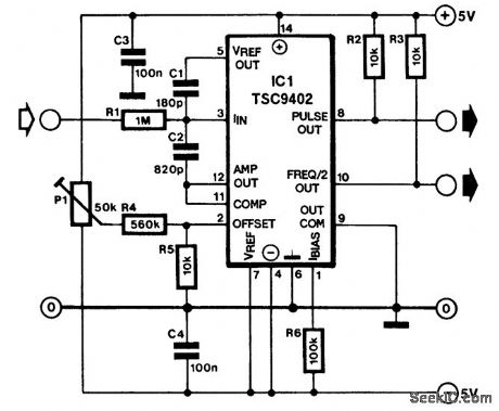
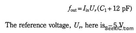
Teledyne Semiconductor's Type TSC9402 IC is eminently suitable as an mexpenstve current-to-fre-quency converter. The maximum input current of the design shown in the diagram is 10 μA (input voltage range is 10 mV to 10 V), while the output frequency range extends from 10 Hz to 10 kHz. The conversion factor is exactly 1 kHz/μA. The factor can be altered by changing the value of R1-as long as the maximum input current of 10 μA is not exceeded.
The circuit has two outputs. That at pin 8 is a short-duration pulse, whose rate is directly proportional to the input current; that zit pin 10 is a square wave of half the frequency of the pulse at pin 8.
Calibrating the circuit is fairly simple. Connect a frequency meter to pin 8 (preferably one that can read tenths of a hertz) and connect a voltage of exactly 10 mV to the input (check with an accurate millivoltmeter). Adjust Pl to obtain an output of exactly 10 Hz. Next, connect a signal of exactly 10 V to the input and check that the output signal has a frequency of 10 kHz. If this frequency cannot be attained, shunt C1 with a small trimmer or replace R1 by a resistor of 820 kΩ and a preset of 250 kΩ.
The circuit may be adapted to individual requirements with the aid of:
(View)
View full Circuit Diagram | Comments | Reading(1719)
PRECISION_FREQUENCY_GENERATOR
Published:2009/7/20 1:43:00 Author:Jessie

Provides 440 cps at 115 v for timing motor of engraved-foil flight recorder. Uses saturating-transformer oscillator and auxiliary regulating circuits to maintain precise voltage and frequency.-H. E. Schauwecker, Dote Recorder for Airplane Flight Analysis, Electronics, 33:48, p 118-120. (View)
View full Circuit Diagram | Comments | Reading(689)
POWER_SAVING_INTERMITTENT_CONVERTER
Published:2009/7/9 23:58:00 Author:May
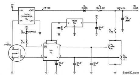
This circuit switches its dc/dc converter, IC1, off whenever the large filter capacitor, C6, has sufficient charge to power the load. This particular circuit uses a dc/dc converter that produces 115 Vdc from a 9-Vdc input; you can tailor the circuit to suit other converters. The heart of the circuit is a 555 timer configured as a dual-limit comparator. Thus, the 555 turns the converter on or off, depending on the voltage across CG. The 555's complementary output lights the charge LED when the FET is on.
Initially, the voltage on CG is zero, and the 555's output turns on the FET, Q1, in turn, enabling the converter to run, which charges C6. When the voltage on the capacitor reaches the value set by R3, the 555 turns the converter off. Then, C6 slowly discharges into the combined load of the voltage divider (R2, R3, and R4) and the reverse-biased blocking diode, D1.
When the voltage falls below 1/3 VCC, the 555 restarts the dc/dc converter. If this circuit powers a load that periodically goes into a zero-power, shutdown mode, the 555 switches the dc/dc converter on full time whenever the load kicks in.
When the supply voltage falls below 7.5 V, the output of the converter is no longer high enough to charge, the LED doesn't light. The circuit uses 205 mA when the converter is on and 10 mA when the converter is off. The duty cycle comprises a 5-s ON period, a 150-s OFF period, and it represents a 92% power reduction. You can further reduce power consumption by removing the charge LED and using a CMOS 555 and a CMOS 78LO5 regulator. (View)
View full Circuit Diagram | Comments | Reading(1077)
FAST_BINARY_ADDING_CIRCUITS
Published:2009/7/9 23:50:00 Author:May
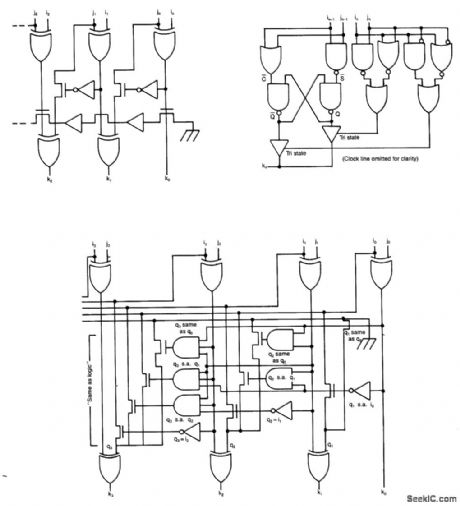
Some circuits that add binary numbers have problems with time delay caused by carry propagation.This has been partially solved by the carry look-ahead adder. However, because of the complexity of this scheme, the carry look-ahead logic usually covers no more than 4 bits, and a ripple carry is implemented between the carry look-ahead blocks.
The Daniels Adder avoids these problems by presenting a scheme where carry bits are not used at all in the process of binary addition. It is based on recognition patterns, which exist with the binary addition truth table.
The addition is described by the following two sets of equations:
if in-1=jn-1 qn=in-1if in-1=jn-1 qn=qn-1if in=jnkn=qnif in=jn kn=qn
with the boundary condition that q-1=0, where in,jn and kn are the bit of binary weight 2n (nth bit) of the addend, summand, and sum respectively, qn is an intermediate variable and qn is the inverse of qn.
The value of the sum is (depending upon in, and jn) either the same as or the inverse of (depending upon in-1 and jn-1) a0, a1, or the inverse of the (n-1)th bit of the sum. Figure 45-1(a) shows the logic diagram of the ripple through implementation of the adder.
Because each stage calculates whether its value of the intermediate variable qn is the same as the previous stage's value (qn-1) in parallel, it is possible to devise simple same as logic that does not have the complexity drawback of carry look-ahead logic and can be carried over any number of bits (Fig.45-1(b)). A 32-bit adder built in this way will result in 11-gate delays (no gate having more than 4 inputs).
Especially compact and efflcient is the pipelined implementation (Fig. 45-1(c)), which can produce the sum at a rate of 3-gate delays/bit.
The high-speed adder circuits can be used on gate arrays or full-custom ICs to implement fast calcula-tion of addresses or data values. Because of their compact nature, they also use less space on the silicon than conventional adders do. (View)
View full Circuit Diagram | Comments | Reading(1909)
EFFICIENT_POWER_BOOSTER
Published:2009/7/9 23:50:00 Author:May

This power booster functions as a high-efficiency power multiplexer or, if you supply an external signal-source, as a high-power linear amplifier.
If you want to drive a load with a high-power square wave, the circuit simply draws power from two external power sources, V1 and V2, alternately. In this mode, the circuit's power-handling devices func-tion as switches, dissipating minimal power. The RC time constant of the integrator,IC1, determines the circuit's oscillation period.
If you supply an external drive waveform, the circuit functions as a linear amplifier,and,consequently, inherently dissipates varying portions of that power. The power amplifier is stable for gains ≥15.
Diodes D1 and D2 limit the FET's gate-voltage swing to less than 15 V. D3 is a dual Schottky diode that protects the FETs from short circuits between the two supplies, V1 and V2, through a FET's para-sitic diode. With D3 in place, you can choose either power channel for the higher voltage input. To drive the FETs, Q5 and Q6, at switching frequencies greater than 1 KHz, you will have to use gate drivers for them. (View)
View full Circuit Diagram | Comments | Reading(658)
4_TO_20_mA_CURRENT_LOOP
Published:2009/7/9 23:49:00 Author:May
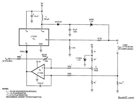
This 5-V circuit utilizesa servo-controlled dc/dc converter to generate the compliance voltage necessary for loop-current requirements. This circuit will drive 4 to 20 mA into loads as high as 2200Ω with 44 V of compliance. It is inherently short-circuit protected. A current source by definition limits current regardless of the load.
The circuit's input voltage and the 4-mA trim network determine 101's positive input voltage. IC1's output biases the LT1072 switching regulator's VC pin, The resistors connected to the regulator's feedback pin, BB, prevent the circuit output from running away in the event that the load opens up.
Normally, IC1 controls the loop. However, if the load opens, IC1 receives no feedback. Under this condition, the Fs pin becomes active when it equals 1.2 V and forces the loop to close locally around the regulator by activating IC2's internal amplifier. Thus, the circuit automatically changes from a current to a voltage regulator, thereby preventing excessive output voltages. (View)
View full Circuit Diagram | Comments | Reading(934)
DIGITALLY_CONTROLLED_VOLTAGE_REFERENCE
Published:2009/7/9 23:45:00 Author:May
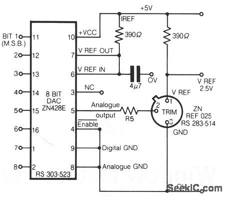
This circuit shows a simple method of achieving a voltage reference which can be trimmed using an 8-bit DAC with an on-chip voltage reference. The analogue output from the DAC drives the trim pin of the ZNREF025 via a resistor, RS. When RS = 0, this circuit will produce a trim range exceeding ± 5% of the nominal reference voltage. When RS is greater than zero, the trim range is reduced. It was found that after dividing the trim range by two, the needed value for RS was approximately 1 MΩ.The reference voltage of the ZNREF025 can be set to an accuracy determined by the trim range of the device itself and the accuracy of the DAC. Increasing RS reduces the percentage trim range and hence increases the effective voltage resolution. Other voltage references from the ZNREF series can be used with this circuit if other voltages are required. This voltage reference can be used to set the value of VREF to a much tighter tolerance, than the data sheet specification of ± 1%, in a much wider range of operating conditions. Applications could include any system with automatic self-calibration of instrumentation, such as in electronic weighing scales. (View)
View full Circuit Diagram | Comments | Reading(1079)
NOISE_BLANKER
Published:2009/7/9 23:41:00 Author:May
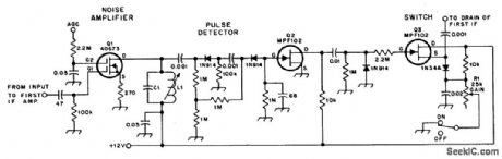
This nolse blanker takes a sample of IF input voltage, amplifies it, and drives a switch, The switch(when activated by a nolse pulse) adds a heavy load to the first IF stage and kills the gam for the pulseduration. (View)
View full Circuit Diagram | Comments | Reading(1963)
WAILING_SIREN
Published:2009/7/9 23:35:00 Author:May

C1 is discharged periodically by uit Q1, which resets voltage controlled oscillator to beginning of its frequency sweep. Controlled oscillator also serves as power amplifier, to reduce number of components required. Circuit draws 10 ma front 9.v bottery.-F. J. Harris, Simple Wailing Siren Circuit, EEE, 14:6, p 94. (View)
View full Circuit Diagram | Comments | Reading(1896)
AUDIO_SHUNT_NOISE_LIMITER
Published:2009/7/9 23:33:00 Author:May
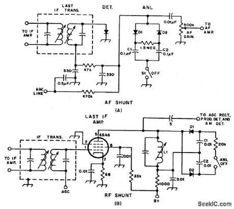
Examples of RF and audio ANL circuits.Positive and negative clipping occurs in both circuits.The circuit at A is self-adjusting.This noise limiter operates at the IF output.It is self-adjusting. Adequate gain is needed at the IF frequency so that several volts p-p of audio is available. (View)
View full Circuit Diagram | Comments | Reading(683)
SAMPLE_AND_HOLD_3
Published:2009/7/9 23:31:00 Author:May
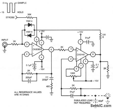
This circuit uses a CA3140 BiMOS op amp as the readout amplifier for the storage capacitor C1, and a CA3080A variable op amp as input buffer amplifier and low feedthrough transmission switch. Offset nulling is accomplished with the CA3140. (View)
View full Circuit Diagram | Comments | Reading(672)
PHONE_RING_REMOTE_CONTROL
Published:2009/7/20 2:33:00 Author:Jessie
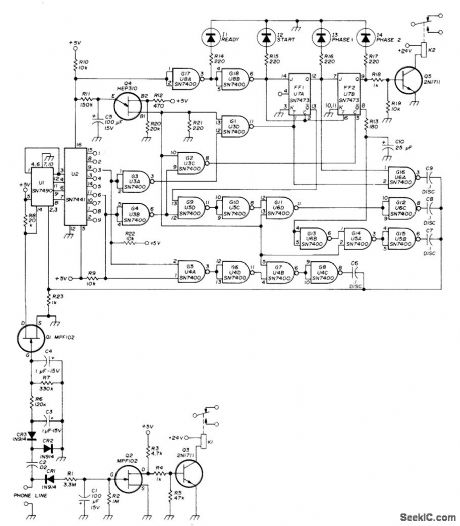
Repeater or other unattended equipment can be turned on or off with ordinary telephone Phone at remote station is called and allowed to ring three times Caller then hangs up, waits 20 s, redials number and lets it ring three times again, then hangs up. Circuit then performs desired control function. Any combination of rings can be used as long as total is less than nine. Decoder U2 is programmed by moving two jumper wires to various outputs of U2. Relay K2 is chosen to give desired momentary, latching, or stepping function. Relay K1 is used for validating phone line, If remote station keying voltage is taken through contacts of K1, interruption of phone line prevents activation of transmitter. C1 stores voltage during brief interruptions such as when phone is ringing. Article gives detailed explanation of ring-counting circuit. LEDs 11-14 indicate status of control sequence and aid in troubleshooting. K1 and K2 are sensitive DPDT relays with 8000-ohm coils. R11 is selected for desired time setting.-R. C. Heptig, Automatic Telephone Controller for Your Repeater, Ham Radio, Nov. 1974, p 44-48. (View)
View full Circuit Diagram | Comments | Reading(944)
SUBAUDIO_TONES
Published:2009/7/20 2:23:00 Author:Jessie
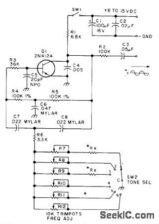
Six-channel subaudible encoder uses twin-T oscillator covering 93 to 170 Hz. Tones are adjustable with 20-turn 10K trimpots. Used with 2-meter amateur transmitters to access and maintain signal through repeater having subaudible tone decoder, When transmitted signal opens up receiver of repeater, subaudible tone on incoming audio closes relay and permits transmitter to key up and repeat signal, Choice of tones permits use of different repeaters in given area. For 93-107 Hz, use 12K for RX; for 98-116 Hz, use 8.2K; and for 114-170 Hz, use jumper. Article gives construction details.-W. G. Moneysmith, Subaudible Tone Encoder, 73 Magazine, Oct. 1977, p 52-53. (View)
View full Circuit Diagram | Comments | Reading(818)
| Pages:216/471 At 20201202203204205206207208209210211212213214215216217218219220Under 20 |
Circuit Categories
power supply circuit
Amplifier Circuit
Basic Circuit
LED and Light Circuit
Sensor Circuit
Signal Processing
Electrical Equipment Circuit
Control Circuit
Remote Control Circuit
A/D-D/A Converter Circuit
Audio Circuit
Measuring and Test Circuit
Communication Circuit
Computer-Related Circuit
555 Circuit
Automotive Circuit
Repairing Circuit