
Index 218
TIME_OUT_WARNING
Published:2009/7/20 2:01:00 Author:Jessie
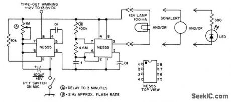
Provides either visual or audible warning after preset interval up to 3 min, when pin 1 of first NE555 is grounded by push-to-talk switch on microphone of mobile transmitter. When preset limit is reached, pin 3 provides ground for second NE555 that makes it pulse at 2-Hz rate to warn that time limit for use of repeater is being approached.-F. Sharp, Time-0ut Warning, QST, 0ct. 1976, p 67. (View)
View full Circuit Diagram | Comments | Reading(708)
DIGITAL_LEVELS_SCOPE_DISPLAYS_2_LOGIC_SIGNALS_ON_1_SCOPE
Published:2009/7/9 23:19:00 Author:May
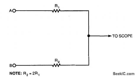
Using this simple resistor circuit, you can trick your oscilloscope into displaying two logic signals on one channel. If you select R2 to be twice R1, the scope trace will show one of four distinct analog levels for each possible combination of the states of inputs A and B.
Of course, the voltage levels that your oscilloscope sees depends heavily on the current-sourcing capability of your digital logic. Because you must use high resistances, this technique has a limited frequency range. (View)
View full Circuit Diagram | Comments | Reading(497)
XOR_GATE
Published:2009/7/9 23:15:00 Author:May
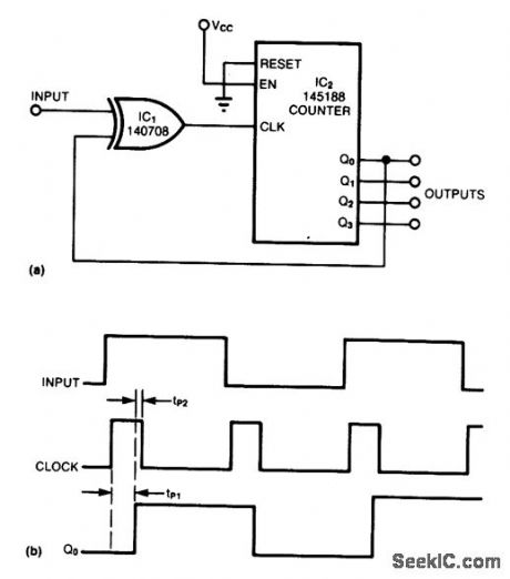
Inverting the negative-going input transactions allows the counter to count both positive- and negative-going edges. The XOR gate transforms the input signal into a series of short pulses whose width is equal to the sum of the counter and gate propagation delays. (View)
View full Circuit Diagram | Comments | Reading(1268)
CODER_MATRIX
Published:2009/7/9 23:15:00 Author:May
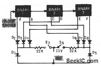
Circuit shows portion of coder matrix associated with microwave system false alarm circuits, having switches 53 and 56.-J. B. Bullock, Pulse-Coded Fauh Alarm in Microwave Systems, Electronics, 33:1, p 82-84. (View)
View full Circuit Diagram | Comments | Reading(593)
SAMPLE_AND_HOLD_2
Published:2009/7/9 23:15:00 Author:May
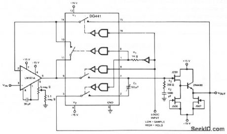
The LM101A provides gain and buffers the input from storage capacitor C2. R2 adds a zero in the open loop response to compensate for the pole caused by the switch resistance and C2, improving the closed-loop stability. R1 provides a slight delay in the digital drive to pins 1 and 9. C1 provides cancellation of coupled charge, keeping the sample-and-hold offset below 5 mV over the analog signal range of -10 through + 10 V. Aperture time is typically 1 pts, the switching time of the DG441. Acquisition time is 25 μs, but this can be improved by using a faster slewing op amp. Droop rate is typically less than 5 mV/s at 25℃. (View)
View full Circuit Diagram | Comments | Reading(819)
AUTOMATIC_LIGHT_BULB_CHANGER
Published:2009/7/9 23:15:00 Author:May
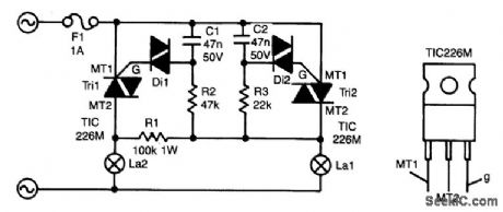
The circuit presented here guarantees that if bulb La1 gives up the ghost, bulb La2 will take over its task. In series with La1 is triac Tri2. Resistor R3 and C2 form a delay network. As soon as the voltage across C2 rises above about 30 V, diac (gateless triac) D2 is switched on, which causes Tri2 to conduct so that La1 lights.
The control circuit of La2 is parallel to that of La1, but because R2/C1 has twice the delay of R3/C2, Tri1 will not be triggered when Tri2 conducts; C1 discharges so that Tri1 cannot be triggered.
When, however, La1 is open-circuited, a voltage is across both RC networks via La2 and RI. Again, Tri2 will be triggered first, but because the current is smaller than its holding current, it will cease to conduct almost immediately. Capacitor C1 will then continue to charge and after a little while Tri1 is switched on.
Because the time constant for La2 is somewhat longer than that for La1, La2 will always be slightly less bright than La1. It is, of course, possible to give La2 a slightly higher wattage than La1 to ensure equal brightness.
Without heatsinks, the triacs can handle up to 100 W each; with heatsinks, powers of up to 1 000W can be accommodated. It is not recommended to use bulbs with a wattage below 25W, because these can flicker.
The triacs can be any type that can handle at least 400 V at no less than 5A. The M types used in the prototype can handle 600 V at 5A. (View)
View full Circuit Diagram | Comments | Reading(1991)
FET_VOLTMETER_1
Published:2009/7/9 23:13:00 Author:May
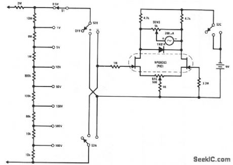
This FETVM replaces the function of the VTVM and rids the instrument of the usual line cord. In addition, FET drift rates are far superior to vacuum tube circuits, allowing a 0.5 V full-scale range which is impractical with most vacuum tubes. The low leakage, low noise NPD8303 is ideal for this application. (View)
View full Circuit Diagram | Comments | Reading(2383)
SAMPLE_AND_HOLD_1
Published:2009/7/9 23:13:00 Author:May
The sample-and-hold function has often been accomplished with separate analog switches and op amps. These designs always involve performance tradeoffs between acquisition time, charge injection, and droop rate. The HA-242-/2425 monolithic sample-and-hold, has many better tradeoffs, and usually a lower total cost than the other ap-proaches. The switching element is a complementary bipolar circuit with feedback, which allows high charging currents of 30 mA, a low charge injection of 10 pC, and an ultra-low off leakage current of 5 pA; a combination that is not approached in any other electronic switch. These factors make it also superior as an integrator reset switch, or as a precision peak detector. (View)
View full Circuit Diagram | Comments | Reading(769)
FUNCTION_DECODER
Published:2009/7/20 2:37:00 Author:Jessie
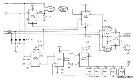
Simple controller for single repeater uses 3-digit control code (523) to turn repeater on and 524 to turn it off. Digits must be in correct sequence. Digit decoder (not shown) uses TTL-compatible inputs which go high when digit is decoded. Four 1N914 diodes form OR gate that triggers U3A to create clock pulse with each digit received. Other output of U3Atriggers 555timer U5, set for delay of about 8 s. At end of delay, timer triggers U3B to reset all logic except for output stage. Regulated VCC of 5 V is obtained from 7805 regulator connected to 12 V.-W. J. Hosking, Simple Sequential Decoder, 73 Magazine, Jan. 1978, p 166-167. (View)
View full Circuit Diagram | Comments | Reading(819)
ALARM_SYSTEM_CODER
Published:2009/7/9 23:12:00 Author:May

Used to generate zone codes for fire alarm.Multivibrator Q3-Q4 determines duration of A and B, while 01-02 delermines lime C-D. Molor-driven stepping switches (not shown) determine the number of K4 operations lo provide predetermined zone coding (zone 1213 for code group shown).-W. F. Ferguson, High-Powered Audio Alarm Systems, Electronics, 33:16, p 70-72. (View)
View full Circuit Diagram | Comments | Reading(645)
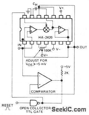
FILTERED_SAMPLE_AND_HOLD
Published:2009/7/9 23:12:00 Author:May
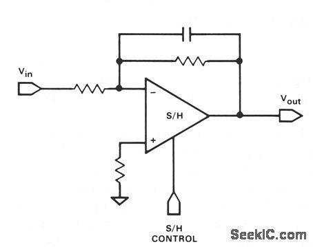
It is often required that a signal be filtered pnor to sampling. This can be accomplished with only one device. Use any of the inverting and noninverting filters that can be built with op amps. However, it is necessary that the sampling switch be closed for a sufficient time for the filter to settle when active filter types are connected around the device. (View)
View full Circuit Diagram | Comments | Reading(790)
1800_Hz_TONE_BURST
Published:2009/7/20 2:35:00 Author:Jessie
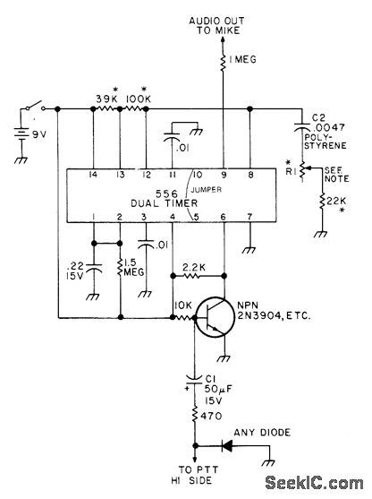
Developed to provide access to repeater requiring accurate tone frequency. Half of 556 dual timer serves as mono MVBR having 0N time of about 400 ms. Other half is free-running oscillator that is disabled when mono goes low. Transistor starts tone burst when push-to-talk switch is closed. For frequency stability, resistors with asterisk should be cermet or wirewound. R1 is 15- or 20-turn trimmer pot having low temperature coefficient and giving about 30 Hz change per turn.-L. Meyer, 0ne IC Tone Burster, 73 Magazine, April 1976, p 55. (View)
View full Circuit Diagram | Comments | Reading(861)
RATE_OF_RISE_HEAT_ALARM_WITH_DELAY
Published:2009/7/9 23:09:00 Author:May
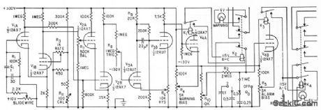
Thermocouple senses rise in temperature of machinery or heat of fire, and feeds servo null-balance recorder having repeater slide-wire. Output of slidewire is differentiated by C1-R1 and compared with reference rise rate voltctge at grid of V1B. When ampliled difference at output of V2 switches Schmitt trigger V3, V4A conducts and energizes K1.Additional triode and relays provide time delay for cdarm lamp.-T. L. Greenwood, Indicalor Warns of Excessive Rise Roles, Electronics, 35:7, p 54-56. (View)
View full Circuit Diagram | Comments | Reading(669)
BASIC_TRACK_AND_HOLD_SAMPLE_AND_HOLD
Published:2009/7/9 23:09:00 Author:May
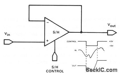
Feedback is the same as a conventional op-amp voltage follower which yields a unity-gain, noninverting output. This hookup also has a very high input impedance. The only difference between a track-and-hold and a sample-and-hold is the time period during which the switch is closed. In track-and-hold operation, the switch is closed for a relatively long period; the output signal might change appreciably and would hold the level present at the instant the switch is opened. In sample-and-ho1d operation, the switch is closed only for the time necessary to fully charge the holding capacitor. (View)
View full Circuit Diagram | Comments | Reading(1092)
SAMPLE_AND_HOLD
Published:2009/7/9 23:07:00 Author:May
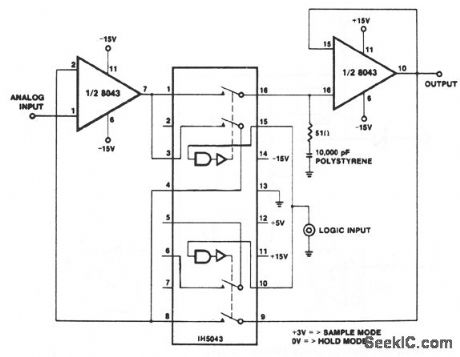
Two important properties of the 8043 are used to advantage in this circuit. The low input bias currents give rise to slow output decay rates (droop) in the hold mode, while the high slew rate at 6 V/μs improves the tracking speed and the response time of the circuit. The upper waveform is the input 10 V/div, the lower waveform the output 5 V/div. The logic input is high.The center waveform is the analog input, a ramp moving at about 67 V/ms, the lower waveform is the logic input to the sample-and-hold; a logic 1 initiates the sample mode. The upper waveform is the output, displaced by about one scope division 2 V from the input to avoid superimposing traces. The hold mode, during which the output remains constant, is clearly visible. At the beginning of a sample period, the output takes about 8 μs to catch up with the input, after which it tracks, until the next hold period. (View)
View full Circuit Diagram | Comments | Reading(0)
SWITCH_BEBOUNCER
Published:2009/7/9 23:07:00 Author:May
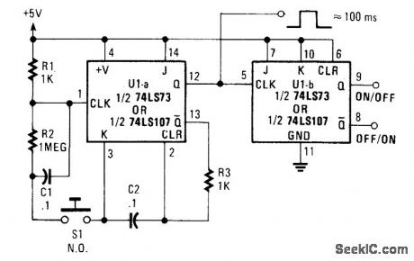
Using a 7473 JK flip-flop U1A connected as a monostable to drive U1B, as a switch debouncer. The circuit is self-clearing during power up. A 100-ms pulse is available at pin 12 U1A. (View)
View full Circuit Diagram | Comments | Reading(992)
POWER_FAILURE
Published:2009/7/9 23:06:00 Author:May
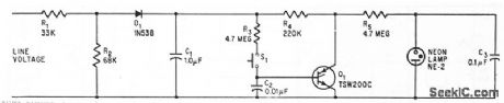
Current of 0.5 ma through R4 holds scr Q1 on normcdly. After power failure, scr will not fire again because it has no gate current. tine voltage across scr then makes neon relaxation oscillctor fiash warning signcal. Depressing S1 resets drcuit.-R.K. Honeycuff, SCR Monitors Electronics, 38:15, p 63. (View)
View full Circuit Diagram | Comments | Reading(694)
QUARTER_STEP_STEPPER_MOTOR_DRIVER
Published:2009/7/9 23:06:00 Author:May
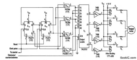
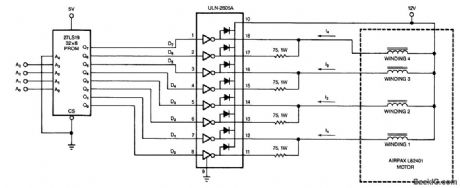
Using a counter and a PROM, this circuit drives the stepper windings with two levels of current. (View)
View full Circuit Diagram | Comments | Reading(907)
POSITIONING_AND_ATTENUATING_CONTROL
Published:2009/7/20 1:59:00 Author:Jessie
Adds d-c positioning voltage lo input signal of recording galvanometer. Magnitudes of input and positioning voltages can be varied independently without interaction. Circuit also has attenuating control for signal voltage.-N. Kassowitz, Non-Interacting Positioning and Attenuating Controls, EEE, 13:3, p 47. (View)
View full Circuit Diagram | Comments | Reading(499)
TIMING_SIGNAL_PLAYBACK
Published:2009/7/20 1:56:00 Author:Jessie
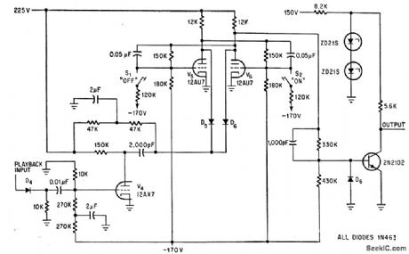
Timing signals, recorded as 50-v negative pulses, each corresponding to an edge of original interval-timing pulse in biomedical experiments, are converted to original rectangular pulse by pulse amplifier and bistable circuit. Negative pulse change state of bistable, to reproduce original pulse at output.-G. Silverman, Modified Tape Recorder Stores Timing Signals, Electronics, 39:13, p 75-76. (View)
View full Circuit Diagram | Comments | Reading(524)
| Pages:218/471 At 20201202203204205206207208209210211212213214215216217218219220Under 20 |
Circuit Categories
power supply circuit
Amplifier Circuit
Basic Circuit
LED and Light Circuit
Sensor Circuit
Signal Processing
Electrical Equipment Circuit
Control Circuit
Remote Control Circuit
A/D-D/A Converter Circuit
Audio Circuit
Measuring and Test Circuit
Communication Circuit
Computer-Related Circuit
555 Circuit
Automotive Circuit
Repairing Circuit