
power supply circuit
Index 110
DC_meter_protection_circui
Published:2009/7/19 20:23:00 Author:Jessie
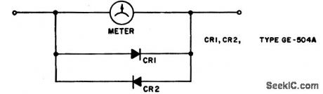
DC meter protection circuit. The diodes will not conduct until the voltage across the meter reaches 0.5 to 0.7 volts. For a typical meter movement with an internal resistance of 1200 ohms and a full-scale current rating of 50 μA the rectifiers will introduce less than 1% error (courtesy General Electric Company). (View)
View full Circuit Diagram | Comments | Reading(919)
Watt_hour_meter
Published:2009/7/19 20:23:00 Author:Jessie
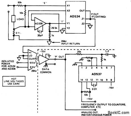
Watt-hour meter. The output of the 284J represents the instantaneous power delivered to the load, which is a 40-watt light bulb. This signal is averaged and converted to a frequency by the AD537 V/F converter. The pulse repetition rate of be AD537 varies in direct proportion to the average power consumed by the 40-watt light bulb. Different sensitivities (e.g., watt-minutes, watt-seconds, etc.) can be obtained by altering the scale factor of the AD537, the gain of the 284J or the count ratio on the AD537 output. lf an analog output is desired, an analog integrator can be successfully employed within the limitations shown (courtesy Analog Devices, Inc.). (View)
View full Circuit Diagram | Comments | Reading(1949)
Sample_and_hold_circuit_with_Av_=_1___RF_RL
Published:2009/7/19 20:21:00 Author:Jessie
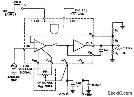
Sample-and-hold circuit with Av = (1 + RF/RL). Circuitry inside dashed lines is the AD582 sample-and-hold amplifier (courtesy Analog Devices, Inc.). (View)
View full Circuit Diagram | Comments | Reading(1511)
High_speed_sample_and_hold_circuit_using_an_ECG915_operational_amplifier
Published:2009/7/19 20:20:00 Author:Jessie
High-speed sample-and-hold circuit using an ECG915 operational amplifier (courtesy GTE Sylvania Incorporated). (View)
View full Circuit Diagram | Comments | Reading(677)
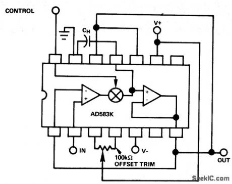
Noninverting_unity_gain_sample_and_hold_circuit_using_a_Datel_SHM_IC_1
Published:2009/7/19 20:19:00 Author:Jessie
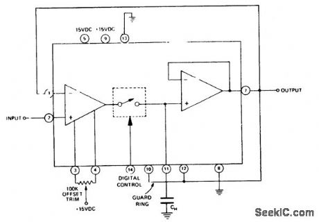
Noninverting unity-gain sample-and-hold circuit using a Datel SHM-IC-1. The SHM-IC-1 is a 14-pin DIP with a 2 MHz bandwidth. The 100 K offset pot should be a 100 PPM/℃ 15-turn type, available from Datel. To zero ground pin 2 and pin 14, then adjust offset for zero output at pin 7 (courtesy Datel Systems, Inc.). (View)
View full Circuit Diagram | Comments | Reading(890)
ELECTRONIC_SHUTDOWN
Published:2009/7/19 20:19:00 Author:Jessie
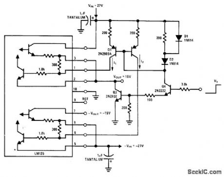
Both sections of National LM125 dual tracking regulatorare shut down by TEL-compatible control signal VT which shorts internal reference voltage of reg-ulatorto ground. Q3 acts only as current sink.-T. Smathers and N. Sevastopoulos, LM125/ LM126/LM127 Precision Dual Tracking Regula-tors, National Semiconductor, Santa Clara, CA, 1974, AN-82, p 15. (View)
View full Circuit Diagram | Comments | Reading(797)
Noninverting_sample_and_hold_circuit_with_gain_equal_to_1__R2_R1
Published:2009/7/19 20:18:00 Author:Jessie
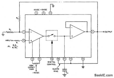
Noninverting sample-and-hold circuit with gain equal to 1 +(R2/R1). The chip is a Datel SHM-IC-1 14-pin DIP. Bandwidth decreases proportionally with gain. R3 is equal to the parallel combination of R1 and R2, and is used to compensate for voltage offset caused by input bias current. R1 and R2 should be 100 PPM/℃ metal film resistors (courtesy Datel Systems, Inc.). (View)
View full Circuit Diagram | Comments | Reading(900)
0_TO_166_V_TRACKING_AT_5_mA
Published:2009/7/19 20:17:00 Author:Jessie
Master-slave regulator combination is used to make second regulator provide mirror image of first wllile output of first is varied over full range from 0 to zener limit with R4. Accuracy of tracking de-pends on match between R5 and R6, which should be1 % film or wirewound.-W. G. Jung, IC Op-Amp Cookbook, Howard W. Sams, Indianapolis, IN, 1974, p 160-162. (View)
View full Circuit Diagram | Comments | Reading(723)
Inverting_sample_and_hold_circuit_with_gain_equal_to__R2_R1
Published:2009/7/19 20:16:00 Author:Jessie
Inverting sample-and-hold circuit with gain equal to -R2/R1. The chip used is a Datel SHM-C-114-pin DIP. For a gain of-1 the bandwidth is one-half of that for the noninverting mode.R3 is equal to the parallel combination of R1 and R2 and is used to compensate for voltage offset caused by input bias current, R1 and R2 should be 100 PPM/℃ metal film resistors for a gain of -1. For high gains the ratio should be matched closely or trimmed with a small value carbon composition type resistor (courtesy Datel Systems, Inc.). (View)
View full Circuit Diagram | Comments | Reading(680)
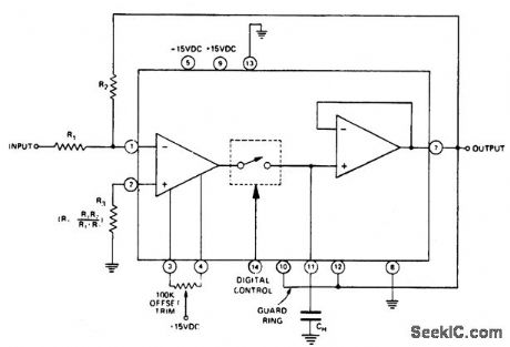
Sample_and_hold_circuit_with_unity_gain_and_offset_nulling
Published:2009/7/19 20:14:00 Author:Jessie
Sample-and-hold circuit with unity gain and offset nulling(courtesy Analog Devices, Inc.). (View)
View full Circuit Diagram | Comments | Reading(811)
5V_AT_10A_WITH_CURRENT_LIMITING
Published:2009/7/19 20:13:00 Author:Jessie
Combination of three transistors and SN52105 or SN72305 regulator provides foldback current limiting for overload protection. Input voltage can be up to 40 V greater than 5-V output. Load regulation is about 0.1%, and input regulation is 0.1%/V.Regulators are interchangeable with LM105 and LM305 respectively.- The Linear and Interface Circuits Data Book for Design Engineers, Texas Instruments, Dallas, TX, 1973, p 5-9. (View)
View full Circuit Diagram | Comments | Reading(1825)
DUAL_OUTPUTS_WITH_TRIMMING
Published:2009/7/19 20:10:00 Author:Jessie
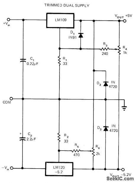
Trimming pots connected across outputs provide positive or negative currents for producing small trimming voltages across 33-ohm ground-leg resistors of National regulators. Same components can be used for higher output voltages, but resistance values of pots should be increased if power dissipation becomes problem.-C. T. Nelson, Power Distribution and Regulation Can Be Simple, Cheap and Rugged, EDN Magazine, Feb. 20, 1973, p 52-58. (View)
View full Circuit Diagram | Comments | Reading(785)
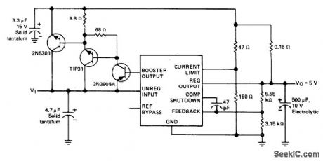
LOW_COST_WITH_DISCRETE_ELEMENTS
Published:2009/7/19 20:09:00 Author:Jessie
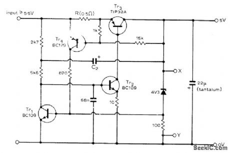
Performance is comparable to that of combined discrete and monolithic circuits, with load regulation of 0.01%, line regulation of 0.05%, ripple rejection of 0.1%, and output ripple and noise of 1 mV. Output is 1 A at 5 V. Foldback short-circuit protection is provided by Tr4, with maximum current determined by value of R. C2, which can be 100 μF, gives extra ripple rejection by introducing more AC feedback into loop.TIP32A is plastic series transistor, and is not critical; many other types will work equally well.-K. W. Mitchell, High Performance Voltage Regulator, Wireless World, May 1976, p 83-84. (View)
View full Circuit Diagram | Comments | Reading(950)
RIPPLE_PREAMP_SUPPLY
Published:2009/7/19 20:07:00 Author:Jessie
Shunt regulator re-moves virtually all AC line ripple without using large capacitor, making it ideal for audio applications where freedom from ripple is more important than precise supply voltage level. Circuit cannot be damaged by short-circuits. Tr3 may be power transistor or Darlington.-P. S. Bright, Ripple Eliminator, Wireless World, April 1977, p 62.
(View)
View full Circuit Diagram | Comments | Reading(963)
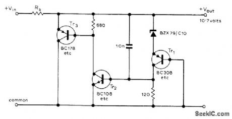
_10_TO__25V_AT_100mA
Published:2009/7/19 20:04:00 Author:Jessie
Series regulator uses opamp as differential amplifier and extra transistor Q2 as current limiter. When 100 mA is drawn, 0.6 V is developed across R2 to make Q2 conduct, pulling al base in negative direction. This action prevents excessive current from being passed by Q1.-H. Olson, Power-Supply Servicing, Ham Radio, Nov. 1976, p 44-50. (View)
View full Circuit Diagram | Comments | Reading(913)
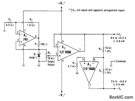
0_15V_AT_2A
Published:2009/7/19 19:57:00 Author:Jessie
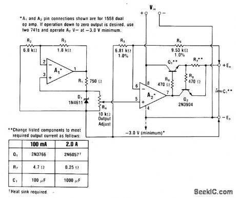
Basic zener-opamp regulator output of 6.6V is scaled up to maximum of 15 V, adjusted with R4, by adding buffer opamp A2, and current-hoosting transistors. Q2 provides short-circuit protection by sensing load current through R7. Large output capacitor C1, maintains low output impedance at high frequencies where gain of A2, falls off.-W. G. Jung, IC 0p-Amp Cookbook, Howard W. Sams, Indianapolis, IN, 1974, p 158-159. (View)
View full Circuit Diagram | Comments | Reading(921)
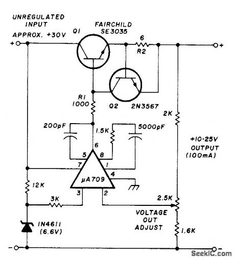
01_24V_AT_1A
Published:2009/7/19 19:55:00 Author:Jessie
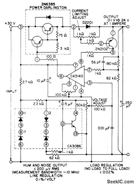
High4mpedance reference-voltage divider across 30-V supply serves CA3140 connected as noninverting power opamp with gain of 3.2. 8-V reference input gives maximum output voltage of about 25V. D2201 high-speed diode serves as current sensor for 2N2102 current-limit sensing amplifier. Current-limiting point can be adjusted over range of 10 mA to 1 A with single 1k pot. Power Darlington serves as series-pass element.- Linear Integrated Circuits and MOS/FET's, RCA Solid State Division, Somerville, NJ, 1977, p 248-256. (View)
View full Circuit Diagram | Comments | Reading(1779)
GATE_CAPACITOR_PROTECTS_SCS_AGAINSTRFI
Published:2009/7/17 23:03:00 Author:Jessie
Capacitor between gate and cathode provides shunt path at higher frequencies to prevent firing of silicon controlled switch by r-f interference. Values in circuit will give protection from 32-V signals between 100 kc and 30 Mc. –R. J. Sanford, Can RFI Control Prevent Weapons Failures?, Electronics, 36:45, p 43-45. (View)
View full Circuit Diagram | Comments | Reading(584)
SOUND_LEVEL_METER
Published:2009/7/17 22:26:00 Author:Jessie
Two-transistor circuit takes high-impedance microphone feeding compound grounded-collector stage in which collector, emitter load, and biased resistor of Q1 are bootstrapped.-W. V Richings and B. J. White, Transistorized Sound Level Meter, Electronic, 33:25, p 64-66. (View)
View full Circuit Diagram | Comments | Reading(5449)
200_MC_POST_AMPLIFIER_FOR_NOISE_FIGURE_METER
Published:2009/7/17 22:19:00 Author:Jessie
Cascaded common-base connection of germanium mesa transistors gives power gain of 40 db, bandwidth of 25 MC, and a noise figure of 3 db. Used between test jig and Hewlett-Packard 342A noise figure meter for measuring noise figure of transistor at 200 Mc. –Texas Instruments Inc., Solid-State Communications, McGraw-Hill, N. Y., 1966, p 345. (View)
View full Circuit Diagram | Comments | Reading(876)
| Pages:110/291 At 20101102103104105106107108109110111112113114115116117118119120Under 20 |
Circuit Categories
power supply circuit
Amplifier Circuit
Basic Circuit
LED and Light Circuit
Sensor Circuit
Signal Processing
Electrical Equipment Circuit
Control Circuit
Remote Control Circuit
A/D-D/A Converter Circuit
Audio Circuit
Measuring and Test Circuit
Communication Circuit
Computer-Related Circuit
555 Circuit
Automotive Circuit
Repairing Circuit