
power supply circuit
Index 106
COSINE_SQUARED_PULSE_GENERATOR
Published:2009/7/17 4:26:00 Author:Jessie
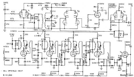
Generates pulse whose width is half the duration. of one input sine-wave cycle. Cosine-squared pulse output is fed into balanced modulator in conjunction with 30-Mc signal, and resulting burst is used as input to synchrodyne, klystron.-K. H. Chase and J. L Pierzga Reducing Mutual Radar Interference, Electronics, 32:28, p 39-43. (View)
View full Circuit Diagram | Comments | Reading(769)
TIMING_PULSE_SHAPER
Published:2009/7/17 4:24:00 Author:Jessie
Monostable mvbr converts timing signal to narrow pulse whose width is accurately controlled by R-C net work. Use of emitter-follower Q4 between triggered transistor Q3 and R-C network assures fast rise and fall times.-C. E. Veazie, Transistorized Radar Sweep Circuits Using Low Power, Electronics, 32:26, p 46-47. (View)
View full Circuit Diagram | Comments | Reading(654)
TUNNEL_DIODE_PARAMETERS
Published:2009/7/17 4:24:00 Author:Jessie
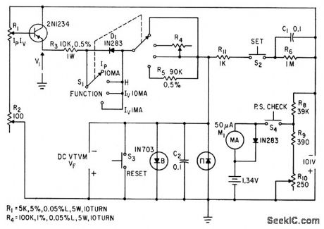
Provides quantitative measurement of all d-c parameters for the three regions of forward d-c characteristic curve for tunnel diodes.-C. D. Todd, Simple Test Sets Measure Tunnel-Diode Parameters, Electronics, 35:14, p 43-45. (View)
View full Circuit Diagram | Comments | Reading(717)
LOGARITHMIC_ATTENUATOR
Published:2009/7/17 4:24:00 Author:Jessie
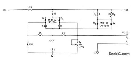
Output of pas sive circuit is proportional to log of input voltages between 0.1 and 100 v. Serves for either positive or negative pulses.-C. D. Nail, Logarithmic Attenuator Spans Three Decades, Electronics, 36:46, p 47-48. (View)
View full Circuit Diagram | Comments | Reading(696)
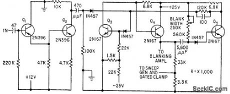
SWEEP_GENERATOR
Published:2009/7/17 4:22:00 Author:Jessie
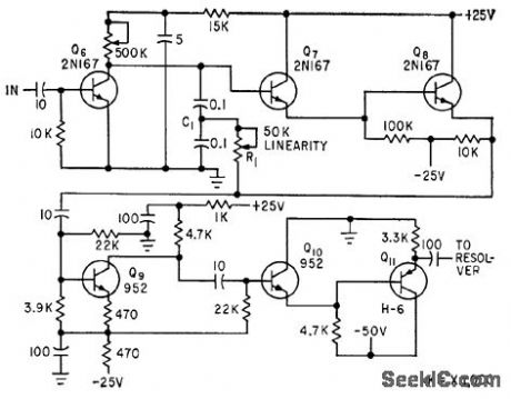
Accepts pulse from monostable mvbr and generates signal for sweep resolver of ppi radar. Voltage rises at constant rate during mono off time, and is held at zero during on time. Cascaded emitter-follower Q7-Q8 provides impedance match to output. Q9-Q10-Q11 provide required power for sweep resolver while preventing thermal runaway at normal temperatures.-C. E. Veazie, Transistorized Radar Sweeps Circuits Using Low Power, Electronics, 32:26, p 46-47. (View)
View full Circuit Diagram | Comments | Reading(2841)
150_MHz_to_300_MHz_frequency_doubler_using_an_MC1596G
Published:2009/7/17 4:21:00 Author:Jessie
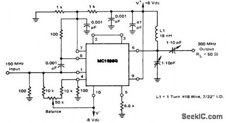
150 MHz to 300 MHz frequency doubler using an MC1596G. Spurious outputs are 20 dB below the desired output (courtesy Motorola Semiconductor Products Inc.). (View)
View full Circuit Diagram | Comments | Reading(700)
Low_frequency_doubler_using_an_MC1596G
Published:2009/7/17 4:20:00 Author:Jessie
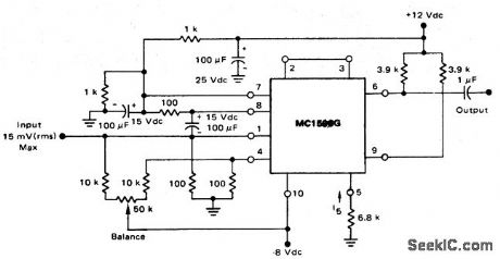
Low-frequency doubler using an MC1596G. This circuit works well in the low-frequency and audio range below 1 MHz (courtesy Motorola Semiconductor Products Inc.). (View)
View full Circuit Diagram | Comments | Reading(828)
±5_V_AND_±12_V
Published:2009/7/17 4:19:00 Author:Jessie

Four different National voltage regulators provide voltages required for wide-range function generator. Power transformer is Triad F90X. - R. C. Dobkin, Wide Range Function Generator, National Semiconductor, Santa Clara, CA, 1974, AN-115. (View)
View full Circuit Diagram | Comments | Reading(682)
DISTANCE_MARK_GENERATOR
Published:2009/7/17 4:19:00 Author:Jessie
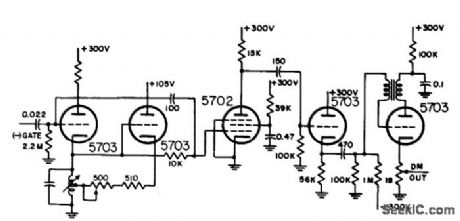
Uses switched Hartley oscillator, pentode amplifier-shaper, and series-triggered blocking oscillator to generate 20-mile distance marks in airborne search radar.-NBS, Handbook Preferred Circuits Navy Aeronautical Electronic Equipment, Vol. 1, Electron Tube Circuits, 1963, p N8-2. (View)
View full Circuit Diagram | Comments | Reading(664)
HYBRID_30_MC_I_F
Published:2009/7/17 4:18:00 Author:Jessie
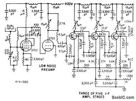
Bandwidth is 6 Mc, noise figure is below 2.5 db, and gain is enough to give 1 V peak-to-peak noise output into 1,000-ohm load when using two transistorzed video stages following the five transistorized i-f gain stages.-J. Scott, D. Randise, and R. P. Lukacovic, Portable Radar Traces Battlefield Deployment, Electronics, 33:12, p 67-70. (View)
View full Circuit Diagram | Comments | Reading(697)
Frequency_doubler_with_linear_amplitude_response_
Published:2009/7/17 4:16:00 Author:Jessie
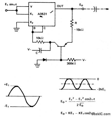
Frequency doubler with linear amplitude response (courtesy Analog Devices, Inc.). (View)
View full Circuit Diagram | Comments | Reading(930)
One_shot_multivibrator_using_a_UJT_1
Published:2009/7/17 4:14:00 Author:Jessie
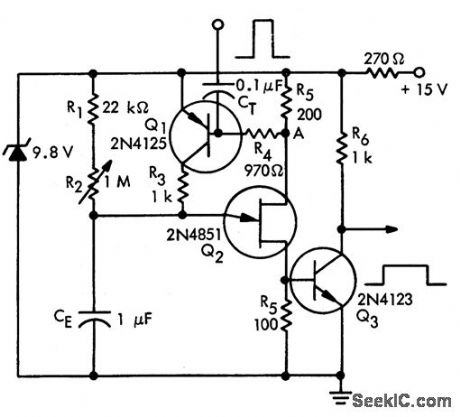
One-shot multivibrator using a UJT (courtesy Motorola Semiconductor Products Inc.). (View)
View full Circuit Diagram | Comments | Reading(748)
SIMPLE_LCD_DISPLAY_POWER_SUPPLY
Published:2009/7/10 21:12:00 Author:May
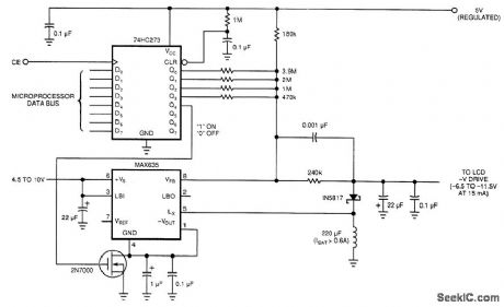
Laptop computers often use large-screen LCDs, which require a variable and a negative supply to ensure maximum contrast. This circuit operates from the system's positive battery supply and generates a digitally variable negative voltage to drive the display.
This figure's switching regulator creates a negative voltage from the battery supply. The microproces-sor data bus drives a 4-bit DAC, which in turn varies the actual regulator output from -6.5 to -11.5 V. This arrangement allows a staircase of 16 possble voltages between these limits.the DAC by using the rail-to-rerail output-drive capability of a 74 HC-series CMOS gate. A resistor divider network formed by the 240-kΩ resistor, connected to the -V filter capadtor and the resistors, is refer-enced to the 5-V supply control (the MAX635 regulator).
When the voltage at the VfB pin is greater than ground, the switching regulator turns on. The inductor dumps this energy into the -V filter capacitor. When the voltage at VFB is less than ground, the regulator skips a cycle. The MAX635 regulates the voltage at the junction of the resistor divider to 0 V. Thus, any resistor that the DAC connects to ground (logic 0) will not contribute any current to the ladder. Only the resistors that are at 5 V (logic 1) will be part of the voltage-divider equation.The entire switching-regulator supply draws less than 150 uA. You can place the circuit in an even lower power mode by interrupting the ground pin. The high-current path is from the battery input through the internal power PMOSFET to the external inductor. Disconnecting the ground connection simply dis-ables the gate drive to the FET and turns off the internal oscillator. (View)
View full Circuit Diagram | Comments | Reading(808)
0_T0_±15V_INDEPENDENTLY_VARIABLE
Published:2009/7/19 20:45:00 Author:Jessie
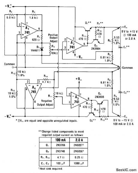
Common zener reference selrves for both regulators. Buffer A3 uses negative reference voltage developed from 6.6-V positive voltage across D1 by inverter A4. Both regulators provide 100mA or 2 A depending on transistors used.-W. G.Jung, IC Op-Amp Cookbook, Howard W. Sams, Indianapolis, IN, 1974, p t62-164. (View)
View full Circuit Diagram | Comments | Reading(770)
Inexpensive_capacitance_meter
Published:2009/7/19 20:44:00 Author:Jessie
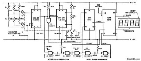
Inexpensive capacitance meter.This circuit uses two 555 timers, or one 556, to generate a gated count for an ICM7217, dependent on the value of capacitance The clock timer operates as a fixed oscillator whose output period is determined by R1, R2 and C. The gating timer also operates as an oscillator, but its output high time is determined by the value of measured capacitance in combination with R3 and R4. Range A reads 1 to 9999 pF, range B reads 1 to 9999 nF, and range B reads 1 to 9999 μF(courtesy Intersil, Inc.). (View)
View full Circuit Diagram | Comments | Reading(5151)
2_35V_VARIABLE
Published:2009/7/19 20:43:00 Author:Jessie
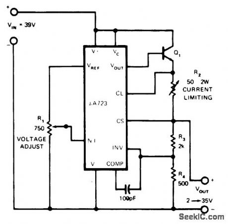
Wide voltage range is achieved by using μA723 regulator IC in simple feedback arrangement requiring only single pot to vary output voltage continuously and linearly from 2 to 35V. Resistors R3 and R4, divide output voltage by 5, so inverting input of regulator sees one-fifth of output voltage. R1 is connected between 7-V reference ofIC and ground to present any intermediate voltage to noninverting input. IC acts to keep these two voltages equal. Maximum input voltage limit is 40V; if possibility of higher voltages exists in lab applications, protect IC with 40-V zener across it.-J. Gangi, Continuously Variable Voltage Regulator, EDN Magazine, Feb. 20, 1973, p 91. (View)
View full Circuit Diagram | Comments | Reading(835)
NARROW_BAND_BALANCED_MODULATOR
Published:2009/7/19 20:40:00 Author:Jessie
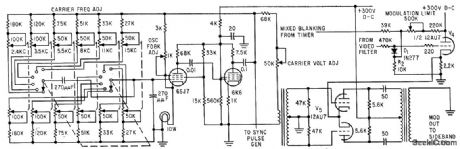
Yields two sidebands and carrier while balancing out original video signal. Gang switch permits use of six different carrier frequencies if sufficient telephone-line band-width is available. Sideband fillers remove upper sideband and part of carrier to provide vestigial sideband operation.-H. W. Gates and A. G. Gatfield, Scan Converter Aids Phone-Line Radar Relay, Electronics, 32:16, p 48-51. (View)
View full Circuit Diagram | Comments | Reading(726)
±5V_AT_10_A_WITH_FOLDBACK_CURRENT_LIMITING
Published:2009/7/19 20:38:00 Author:Jessie
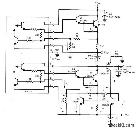
Combination of Darlington pass transistors and current limiting is used with National LM125 dual tracking regulator to give high output currents with protection from short-circuits.-T. Smathers and N. Sevasto-poulos, LM125/LM126/LW127 Precision Dual Tracking Regulators, National Semiconductor, Santa Clara, CA, 1974, AN-82, p 11. (View)
View full Circuit Diagram | Comments | Reading(981)
DISTANCE_MARK_GENERATOR_6
Published:2009/7/19 20:34:00 Author:Jessie
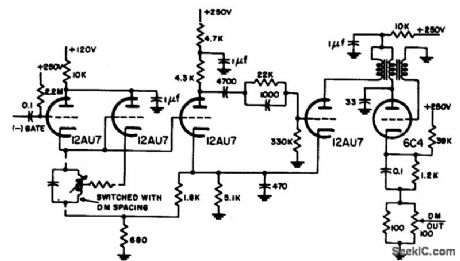
Uses switched Hartley oscillator, monostable mvbr-type trigger shaper, and parallel-triggered blocking oscillator lo generate distance marks for 2, 5, and 25 miles in airborne search radar. RLC unit is switched to change mark spacing.-NBS, Handbook Preferred Circuits Navy Aeronautical Electronic Equipment, Vol. 1, Electron Tube Circuits, 1963, p N8-1. (View)
View full Circuit Diagram | Comments | Reading(692)
28V_AT_1A
Published:2009/7/19 20:34:00 Author:Jessie
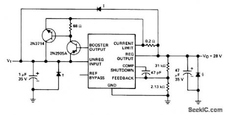
Circuit uses SN52105 or SN72305 regulator with three protective diodes. Feedback diode at top protects against shorted input and inductive loads on unregulated supply. Input diode protects against input voltage reversal. Output diode protects against output voltage reversal. Maximum input voltage is 50V.- The Linear and Interface Circuits Data Book for Design Engineers, Texas Instruments, Dallas, TX, 1973, p 5-9. (View)
View full Circuit Diagram | Comments | Reading(854)
| Pages:106/291 At 20101102103104105106107108109110111112113114115116117118119120Under 20 |
Circuit Categories
power supply circuit
Amplifier Circuit
Basic Circuit
LED and Light Circuit
Sensor Circuit
Signal Processing
Electrical Equipment Circuit
Control Circuit
Remote Control Circuit
A/D-D/A Converter Circuit
Audio Circuit
Measuring and Test Circuit
Communication Circuit
Computer-Related Circuit
555 Circuit
Automotive Circuit
Repairing Circuit