
power supply circuit
Index 119
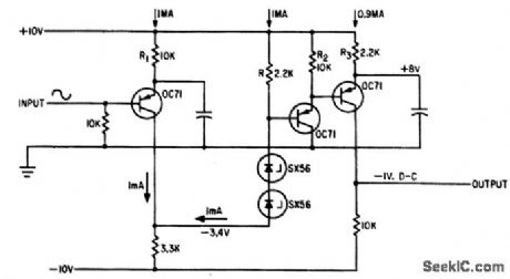
FORMING_ELECTROLYTICS
Published:2009/7/20 2:40:00 Author:Jessie
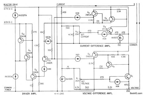
Current-difference amplifier delivers constant current during initial forming of electrolytic capacitors, and voltage-difference amplifier holds voltage constant when final forming voltage is reached. Values of current and voltage can be adjusted over wide range of preset values for different sizes of capacitors.-J. W. Martin and H. Liepins, Unique Power Supply. Delivers Constant Voltage and Current, Electronics, 35:31, p 40-41. (View)
View full Circuit Diagram | Comments | Reading(821)
MAGNETRON_INJECTION_ELECTRODE_SUPPLY
Published:2009/7/20 2:57:00 Author:Jessie
Constclnf-volfc1ge bridge footing on variatble resistor feeds differential amplifier and series regulator. Rheostat setting determines value of regulated output voltage.-S. Prigozy, Designing Special Power Supplies for Voltage-Tunable Oscillators, Electronics, 35:44, p 48-50. (View)
View full Circuit Diagram | Comments | Reading(806)
OVERLOAD_PROTECTION_FOR_SERIES_REGULATOR
Published:2009/7/20 3:12:00 Author:Jessie
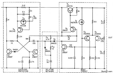
For input voltage of 30 to 40 v d-c, output at full load of 3 amp will be held within 99.09% of 28 v. Tunnel diode D4 and transistor Q8 in overload-sensing circuit trigger monostable mvbr Q6-Q7 to remove drive from Q1 until mvbr resets.-J.Takesuye, Tunnel-Diode Sensor Protects Regulator from Short Circuit, Electronics, 38:25, p 75-76. (View)
View full Circuit Diagram | Comments | Reading(888)
TUBE_ZENER_REGULATOR
Published:2009/7/20 3:10:00 Author:Jessie
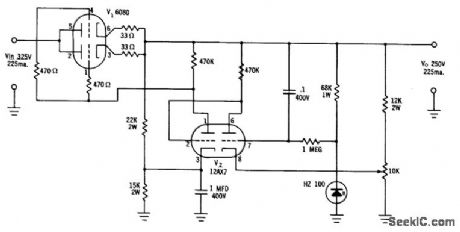
Regulates within 0.2 v from no load lo full load. Variation of 10% in line voltage causes only 0.1 v output change.- Zener Diode Handbook, Intenational Rectifier Corp., 1960, p 59. (View)
View full Circuit Diagram | Comments | Reading(906)
LARGE_VOLTAGE_SWING_WITH_WIMITED_SUPPLY_VOLTAGES
Published:2009/7/20 3:08:00 Author:Jessie
Circuit shows usual solution to problem, wherein final transistor is operated near positive supply voltage and zener diode provides coupling. Drop in gain caused by R can be eliminated by using constant-current diode in place of R. If R1, R2, and R3 are similarly replaced with these diodes, circuit becomes independent of positive line, eliminating spurious feedback through this line.-T. K. Hemingway, Applications of the Constant-Current Diode, Electronics, 34:42, p 60-63. (View)
View full Circuit Diagram | Comments | Reading(881)
50_CPS_2_KG_REGULATOR
Published:2009/7/20 3:06:00 Author:Jessie
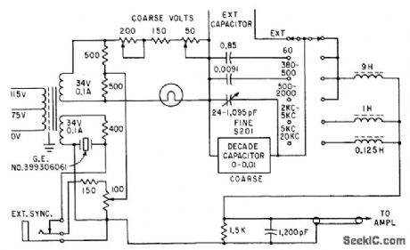
Thermal bridge using ordinary iron-wire ballast tube is used with tunable filler of 200 via variable-frequency power supply for instrument calibration. Output stage (not shown) uses two 7378 pentodes in push-pull class AB1, with positive feedback.-E. A. Gilbert, Precision Variable Frequency Power Supply, Electronics, 34:2, p 99-100. (View)
View full Circuit Diagram | Comments | Reading(702)
BACKWARD_WAVE_OSCILLATOR_FILAMENT_SUPPLY
Published:2009/7/20 3:04:00 Author:Jessie

Provides constant voltage for filament of backward-wave oscillator. Output voltage is compared with fixed reference in d-c amplifier, and difference is used to control series pass element.-S. Prigozy, Designing Special Power Supplies for Voltage Tunable Oscillators, Electronics, 35:44, p 48-50. (View)
View full Circuit Diagram | Comments | Reading(813)
12_V_REGULATED_SUPPLY_WITH_REFERENCE_AMPLIFIER
Published:2009/7/20 3:03:00 Author:Jessie
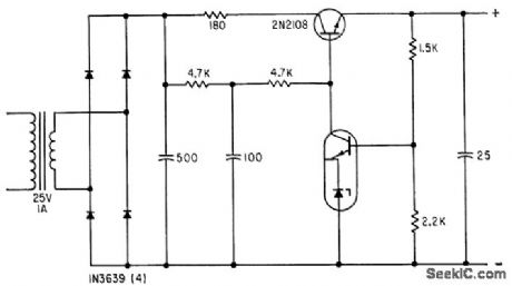
Integrated transistor and zener diode in reference amplifier act with tansistor 2N2108 lo hold 12.v d-c output voltage within 0.3% over ac line voltage variations of 10% for load currents up to 100 ma-T. P. Sylvan, New Device Simplifies Power Supply Design, Electronics, 36:20, p 39-43. (View)
View full Circuit Diagram | Comments | Reading(709)
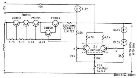
HIGH_CURRENT_REGULATOR
Published:2009/7/20 3:01:00 Author:Jessie
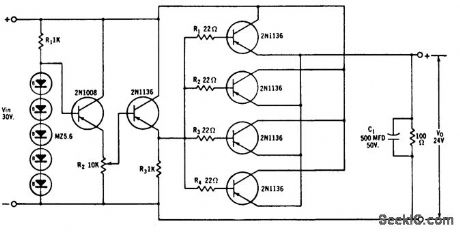
Four parallel-connected transistors handle up to 240 w if mounted with heat sink. If output voltage is reduced, separate power supply must be provided for zener regulator to protect transistors.- Zener Diode Handbook, International Rectifier Corp., 1960, p 57. (View)
View full Circuit Diagram | Comments | Reading(1259)
MAGNETICAMPLIFIER_REGULATOR
Published:2009/7/20 3:00:00 Author:Jessie
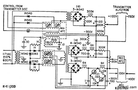
Provides stable operating voltages for transmitter and receiver local-oscillator klystrons in 6,000- Mc microwave link.-M. C. Harp, Nonvacuum Devices Control Klystrons, Electronics 32:7, p 68-70. (View)
View full Circuit Diagram | Comments | Reading(1090)
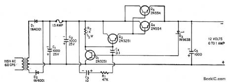
6_V_D_C_REGULATOR
Published:2009/7/20 2:59:00 Author:Jessie
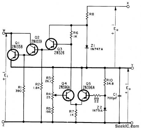
Provides 4 amp at 6 v with 1% regulation for inputs of 7 to 50 v from unregulated source. Auxiliary source Ea must be minimum of 5 v.-NBS, Handbook Preferred Circuits Navy Aeronautical Electronic Equipment, Vo1. 11, Semiconductor Device Circuits, PSC 1, p 1-2. (View)
View full Circuit Diagram | Comments | Reading(826)
300_V_200_MA_REGULATOR
Published:2009/7/20 4:23:00 Author:Jessie
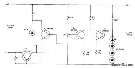
Transistor Q1 serves as series element in negative lead of high-voltage regulated supply, dissipating less than 16 w. Zener Diode Handbook, International Rectifier Corp., 1960, p 58. (View)
View full Circuit Diagram | Comments | Reading(719)
BRIDGE_CIRCUIT_WITH_ONE_POWER_SUPPLY
Published:2009/7/9 21:22:00 Author:May
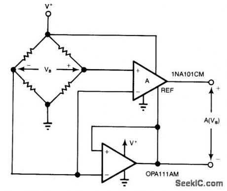
For systems with only one power supply, two op amps act as instrumentation and buffer amps. The OPA111AM buffers the reference mode of the bridge and applies that voltage to the instrumentation amps REF terminal. Output is taken between the amplifier outputs to exclude the fixed output offset.
The additional op amp creates a bridge error of IB x R/2, where IB = bias current of op amp and fi is the resistance of one leg of the bridge. (View)
View full Circuit Diagram | Comments | Reading(777)
LOW_RIPPLE_AT_LOW_COST
Published:2009/7/20 4:21:00 Author:Jessie
Ripple at output is used to control d-c resistance of series regulator transistors Q3-Q4, to keep ripple below 10 my rms over wide temperature range. Cost is under $15.-R. E. Risely, Power Supply Reduces Ripple by Varying Series Resistance, Electronics, 39:2, p 74-75. (View)
View full Circuit Diagram | Comments | Reading(689)
DUAL_POLARITY_15_V_SUPPLY
Published:2009/7/20 4:20:00 Author:Jessie
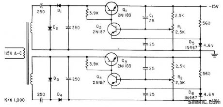
Output voltage is adjustable from 11 to15 v d-c and nearly constant from no load to 300 ma, or from 90 to 140 v ac line voltage.-D. T. Birch and K. E. Challis, Regulated Positive. Negative Supply Delivers Low-Voltage Direct Current, Electronics, 34:30, p 62. (View)
View full Circuit Diagram | Comments | Reading(684)
REGULATED_3_V_SUPPLY
Published:2009/7/20 4:18:00 Author:Jessie
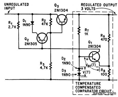
Junction diode D1 provides nonlinear voltage-current characteristic of tenor diode, as required for reference level below 2 v. Poor temperature characteristics of junction diode are offset by base-emitter voltage variation of transistor Q1 with temperature. Regulated output of 3 v within 2%, at 5 to 100 ma, is obtained from unregulated 4.8-v source over range of -16°C to +50°C.-A. K. Scidmore, Junction Diode Regulates Low-Voltage Supply, Electronics, 37:27, p 55-56. (View)
View full Circuit Diagram | Comments | Reading(758)
5_AMP_AT_0_TO_20_V
Published:2009/7/20 4:16:00 Author:Jessie
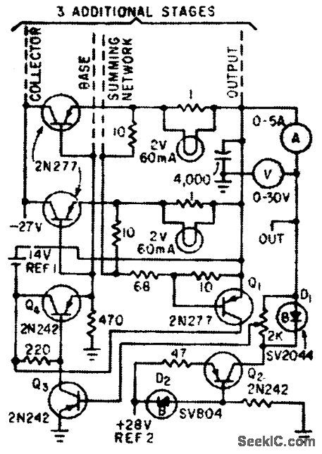
Five regulator transistors in 5-amp power supply have indicator lamps at their emitters. Regulation is better than 0.1% at 20 v, and ripple is below 1 my rms.-J. A. Wheeler and E. J. Currence, Faull-Indicating Series Regulator, Electronics, 34:4, p 60. (View)
View full Circuit Diagram | Comments | Reading(638)
ACCESS_CONTROL_FOR_OPEN_REPEATER
Published:2009/7/20 4:56:00 Author:Jessie
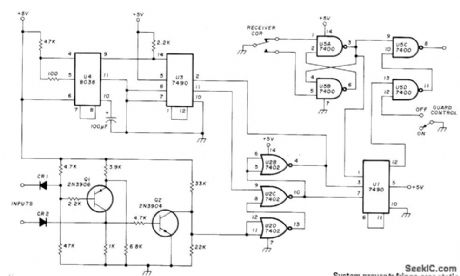
Permits repeater to run open, for user access without access tone, when there is no outside interference on input frequency. Carrier-operated relay (COR) pulse is shaped by 7400 gates U5A and U5B, for keying transmitter through U5C as long as output of U5D is high. (Turning guard control switch off latches output of U5D high, letting repeater run open) When control switch is on, repeater can be accessed only by use of guarded input applied toQ1 such as 2000-Hz tone burst, 1336-Hz Touch-Tone signal, or 110.9-Hz private line. Repeater then remains open for 5s after duration of each transmission. System prevents fringe-area station from blocking repeater access for local users. When receiver squelch is operated 3 times in succession by signal not having one of access tones, input is automatically guarded for 15min by timer U3-U4 unless accepted access tone arrives.-R. B.Shrove, Troubleshooting Logic Circuits, Ham Radio, Feb, 1977, p 56-59. (View)
View full Circuit Diagram | Comments | Reading(1976)
PREFERRED__150_V_D_C_REGULATOR
Published:2009/7/20 4:55:00 Author:Jessie
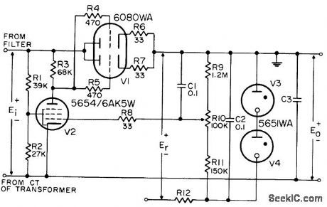
Provides 1% output voltage regulation under normal line and load variations of military equipment. Minimum value of C3 is 2 mfd. Value of R12 depends on reference voltage Er, which should be minimum of -300 v d-c. Two reference tubes, V3 and V4, are used in series so negative bias for V2 can be obtained with grounded reference supply. Minimum input voltage is 200 v d-c.-NBS, Handbook Preferred Circuits Navy Aeronautical Electronic Equipment, Vol. 1, Electron Tube Circuits, 1963, PC 2, p 2-2. (View)
View full Circuit Diagram | Comments | Reading(3064)
1800_Hz_COMMAND_OSCILLATOR
Published:2009/7/20 4:53:00 Author:Jessie
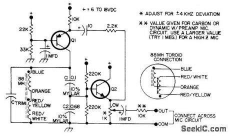
Connects across microphone leads of FM transceiver, to produce control (command) tone for entry to repeater or for other purposes. Switch may be placed in supply lead if desired. Q1 can be 2N404 or one of transistors in 2N1303, 2N2904, 2N3638, 2N6516, or 2N6533 series. Q2 can be 2N1308, 2N2712, 2N3565, 2N3569, 2N6513, or equivalent. CTRIM is 0.0062 μF.-Circuits, 73 Magazine, April1973, p 132. (View)
View full Circuit Diagram | Comments | Reading(2211)
| Pages:119/291 At 20101102103104105106107108109110111112113114115116117118119120Under 20 |
Circuit Categories
power supply circuit
Amplifier Circuit
Basic Circuit
LED and Light Circuit
Sensor Circuit
Signal Processing
Electrical Equipment Circuit
Control Circuit
Remote Control Circuit
A/D-D/A Converter Circuit
Audio Circuit
Measuring and Test Circuit
Communication Circuit
Computer-Related Circuit
555 Circuit
Automotive Circuit
Repairing Circuit